Semiconductor storage device

A storage device and semiconductor technology, applied in the direction of semiconductor devices, information storage, semiconductor/solid-state device manufacturing, etc., can solve the problems of characteristic deviation and large difference, so as to suppress the increase of the area, shorten the length of the bit line, and realize the reduction of the area Effect

Inactive Publication Date: 2012-08-15
SOCIONEXT INC
View PDF6 Cites 4 Cited by
  • Summary
  • Abstract
  • Description
  • Claims
  • Application Information

AI Technical Summary

Problems solved by technology

Especially in the memory cell, not only the memory cell itself has a fine pattern, but also in the memory array in which the same memory cell is arranged across a plurality of wide ranges, the pattern difference between the central part and the end of the memory array is large, so it is easy to produce characteristic deviation

Method used


Image

  • Semiconductor storage device
  • Semiconductor storage device
  • Semiconductor storage device

Examples


no. 1 approach

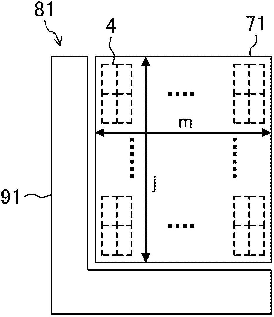
[0034] figure 1 It is a block diagram of ROM81 concerning 1st Embodiment of this invention. exist figure 1 Among them, 71 is a memory array in which the cell patterns 4 are arranged in a matrix (m×j). Wherein, m is the number of cell patterns in the horizontal direction (word line direction), and j is the number of cell patterns in the vertical direction (bit line direction). 91 is a peripheral circuit for outputting data stored in a ROM memory cell, and is connected to the memory array 71 via a word line and a bit line.

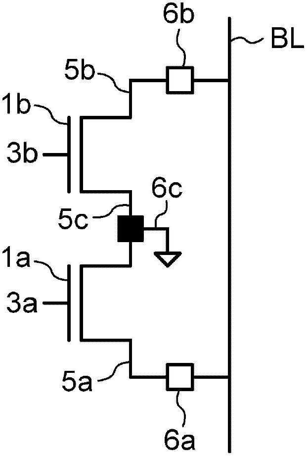
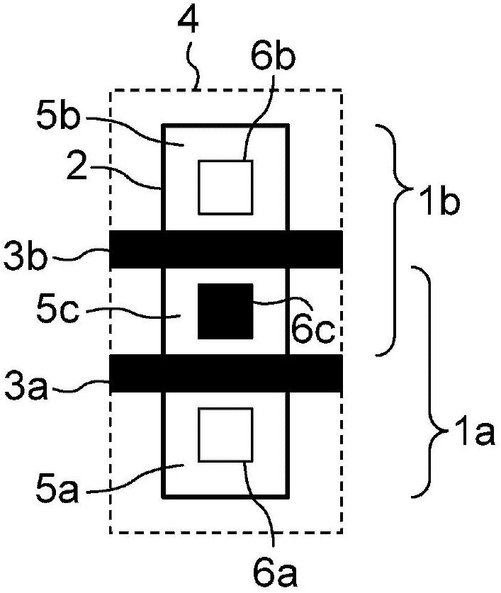
[0035] Figure 2(a) shows figure 1 The circuit diagram of a unit pattern 4 in Fig. 2(b) is its layout pattern diagram. In FIG. 2(a) and FIG. 2(b), 1a and 1b respectively denote N-channel memory cell transistors constituting one ROM memory cell. 2 is a diffusion pattern constituting the memory cell transistors 1a and 1b, and 3a and 3b are gate terminals of the memory cell transistors 1a and 1b, which are connected to word lines. 5a, 5b, and 5c denote dif...

no. 2 approach

[0045] Figure 4 It is a block diagram of a hierarchical bit line structure type ROM 82 having a memory array 72 divided into two arrays according to the second embodiment of the present invention. exist Figure 4 Among them, 72 is a storage array divided into two arrays, ie, a first array 101 and a second array 102 . The first and second arrays 101 and 102 are arrays in which the unit patterns 4 are arranged in a matrix (m×j), respectively. 20 is a logic circuit, which is composed of completely different patterns from the first and second arrays 101, 102, connected to the first and second arrays 101, 102 via bit lines, and the logic circuit 20 is used to control ROM readout, including Amplifier etc.; 92 is the peripheral circuit. The logic circuit 20 outputs stored data to the outside through other wirings.

[0046] Figure 5 yes Figure 4 A detailed layout pattern diagram of the storage array 72 in FIG. Each column of the first array 101 and the second array 102 has b...


PUM


Abstract

In a semiconductor storage device that includes memory cells each constituted by one transistor, two adjacent bits of the memory cells form a diffusion pattern (4), two adjacent transistors share a common source region, and the two drain regions are separated from each other. A plurality of arrays (120, 130) each including at least one line of the diffusion patterns (4) have bit lines that are independent for each array. In addition, end portions of the bit lines for each array are located on the two drain regions separated from each other with the common source regions interposed therebetween in one diffusion pattern (4) at an array-dividing border portion. With this, the area can be reduced while a sufficient separation width between the bit lines can be ensured.

Description

technical field [0001] The present invention relates to an arrangement of a semiconductor memory device. Background technique [0002] Among semiconductor storage devices, a read only memory (ROM) has an important function as a nonvolatile memory whose data does not disappear even if the power is turned off, and is widely mounted on various semiconductor products. Since the memory cell of the ROM can store 1-bit data with one transistor, it is effective in reducing the circuit scale, that is, the area, compared with a static random access memory (SRAM) that requires multiple transistors to store 1-bit data. [0003] In the fine process, there are many causes of variation in pattern formation, and even if the target pattern has the same shape, it is greatly affected by other patterns arranged around it. Especially in the memory cell, not only the memory cell itself has a fine pattern, but also in the memory array in which the same memory cell is arranged across a plurality o...

Claims


Application Information

Patent Timeline
Patent Type & Authority Applications(China)
IPC IPC(8): H01L21/8246G11C16/04H01L27/112
CPCG11C16/0408G11C16/06H10B20/00H10B69/00H10B41/10
Inventor 寺田裕仓田胜一
Owner SOCIONEXT INC
Why Eureka
Try Eureka