Liquid crystal display panel array substrate and manufacturing method thereof
A technology for liquid crystal display panels and array substrates, which is used in semiconductor/solid-state device manufacturing, optics, instruments, etc., and can solve the problems of non-conduction and high contact resistance.
- Summary
- Abstract
- Description
- Claims
- Application Information
AI Technical Summary
Problems solved by technology
Method used
Image


Examples
Embodiment 1
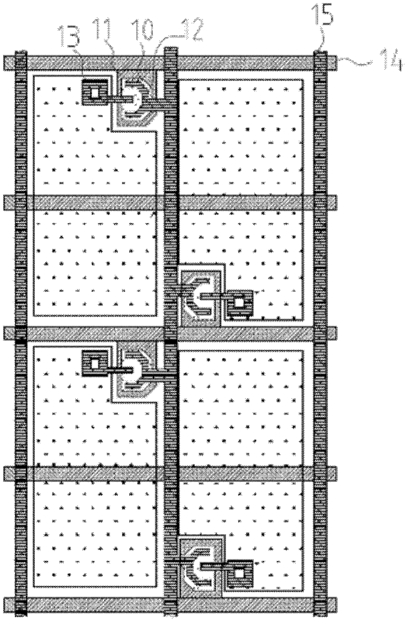
[0038] Example 1, please refer to Figure 5 , Figure 5 A front view of an array substrate of a liquid crystal display panel provided by the present invention, in which a plurality of scanning lines 210 are distributed laterally on the substrate (not shown in the figure), and a plurality of data lines 220 are interlaced with the scanning lines, and the scanning lines and The data lines are criss-crossed to form a plurality of pixels, wherein a plurality of thin film transistors are located at the intersection of the scan line 210 and the data line 220, wherein the scan line 210 is connected to the gate 251, the data line 220 is connected to the source 252, and above the gate 251 There are channel layers 253 overlapping and separated by an insulating layer, and the drain electrode 254 is connected to the pixel electrode 256 through the connection hole 255. In addition, there is a common electrode line 230 parallel to the scanning line 210 and located in the pixel area. Therefo...
no. 2 example
[0042] Another embodiment of the present invention provides a method for fabricating metal wiring on an array substrate of a liquid crystal display panel, such as Figure 7A to Figure 7B As shown, firstly, multiple layers of metal films are continuously deposited on the substrate 200. If the metal wiring is formed directly on the substrate, the substrate 200 is a substrate, such as a glass substrate, a plastic substrate, or other flexible substrates. When the metal wiring is formed on another film layer, the base may be another film layer, such as an insulating film. In this embodiment, taking the substrate as an example, three layers of metal films are continuously deposited on the substrate, wherein the bottom layer is a molybdenum metal film 301, the middle is an aluminum metal film 302, and the uppermost metal layer is a molybdenum metal film. 301 is a molybdenum-aluminum-molybdenum structure. The thickness of the aluminum metal film in the present invention is between 250...
PUM
| Property | Measurement | Unit |
|---|---|---|
| thickness | aaaaa | aaaaa |
| thickness | aaaaa | aaaaa |
Abstract
Description
Claims
Application Information
 - R&D
- Intellectual Property
- Life Sciences
- Materials
- Tech Scout
- Unparalleled Data Quality
- Higher Quality Content
- 60% Fewer Hallucinations
Browse by: Latest US Patents, China's latest patents, Technical Efficacy Thesaurus, Application Domain, Technology Topic, Popular Technical Reports.
© 2025 PatSnap. All rights reserved.Legal|Privacy policy|Modern Slavery Act Transparency Statement|Sitemap|About US| Contact US: help@patsnap.com