
Scanning electron microscope (SEM) sample fixture used in on line SEM observing and SEM sample observing method

A sample observation and sample technology, applied in the direction of material analysis, discharge tube, electrical components, etc. by measuring secondary emissions, can solve the problems that online SEM cannot conduct SEM sample/section observation, high cost, etc.

Active Publication Date: 2012-08-22
SHANGHAI INTEGRATED CIRCUIT RES & DEV CENT
View PDF7 Cites 10 Cited by
  • Summary
  • Abstract
  • Description
  • Claims
  • Application Information

AI Technical Summary

Problems solved by technology

[0005] The purpose of the present invention is to provide a SEM sample fixture and SEM sample observation method for online SEM observation, to solve the problem that the online SEM cannot perform SEM sample / section observation in the prior art, or it needs to be equipped with FIB function, resulting in high cost. question

Method used


Image

  • Scanning electron microscope (SEM) sample fixture used in on line SEM observing and SEM sample observing method
  • Scanning electron microscope (SEM) sample fixture used in on line SEM observing and SEM sample observing method
  • Scanning electron microscope (SEM) sample fixture used in on line SEM observing and SEM sample observing method

Examples


Embodiment 1

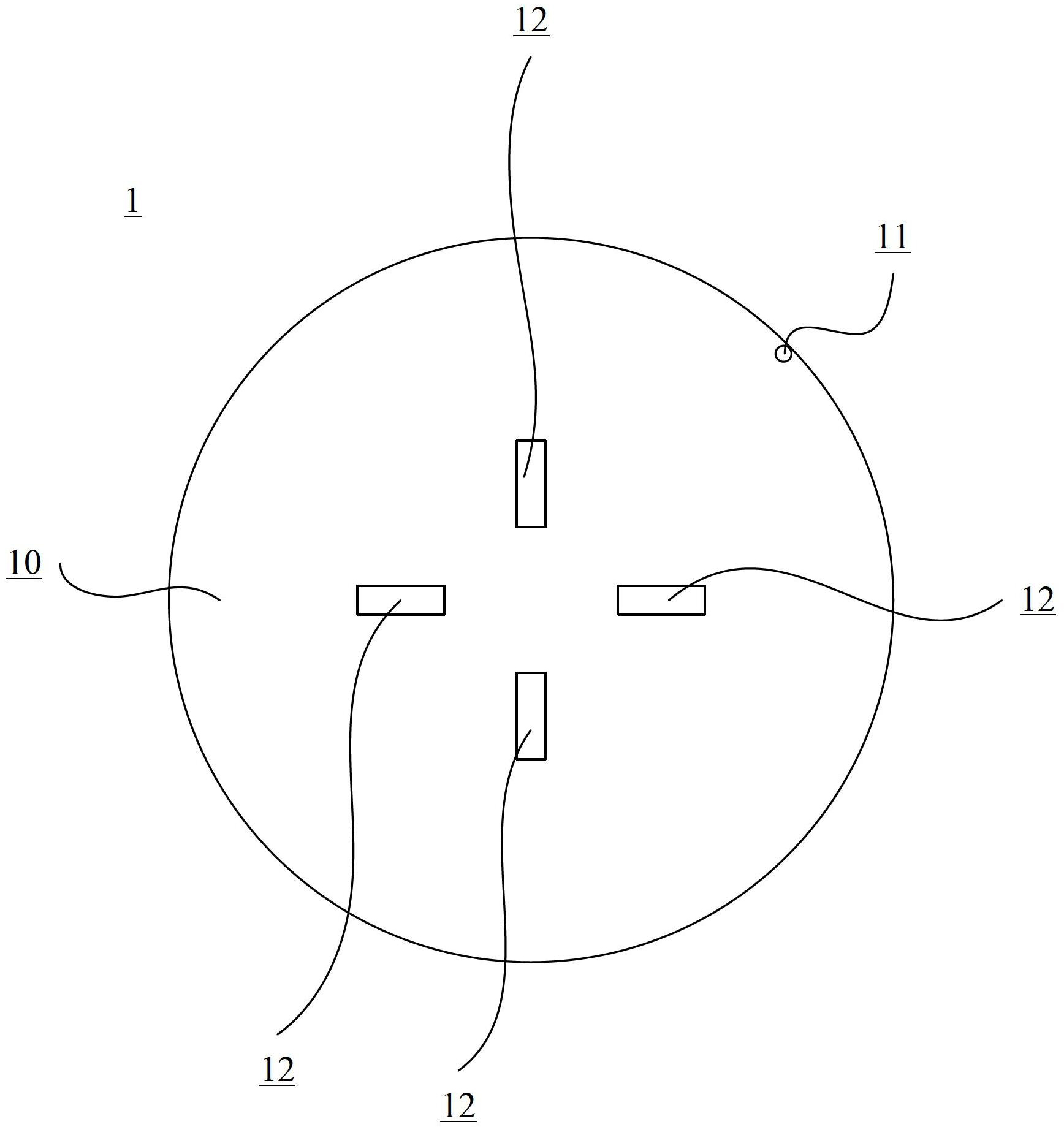
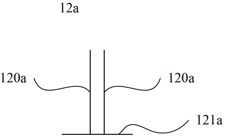
[0048] Please refer to Figure 1a~1b ,in, Figure 1a It is a schematic top view of the SEM sample fixture for online SEM observation according to Embodiment 1 of the present invention; Figure 1bIt is a schematic side view of the SEM sample fixture used for online SEM observation in Example 1 of the present invention.

[0049] like Figure 1a As shown, the SEM sample holder 1 includes:

[0050] A disc-shaped metal support 10, the disc-shaped metal support 10 is provided with a Notch notch 11;

[0051] The disc-shaped metal bracket 10 has one or more grooves 12 .

[0052] Specifically, the disc-shaped metal stent 10 has a diameter of 150 mm to 300 mm and a thickness of 0.4 mm to 6 mm. Usually, the shape of the disc-shaped metal support 10 is equivalent to the size of the wafer on the production line, that is, for example, the wafer on the production line is a 6-inch wafer, then the shape and size of the disc-shaped metal support 10 It is basically the shape and size of a 6-...

Embodiment 2

[0061] Please refer to Figure 3a~3b ,in, Figure 3a It is a schematic bottom view of the SEM sample fixture for online SEM observation according to the second embodiment of the present invention; Figure 3b It is a schematic side view of the SEM sample fixture used for online SEM observation according to the second embodiment of the present invention.

[0062] like Figure 3a As shown, the SEM sample holder 3 includes:

[0063] A disc-shaped metal support 30, the disc-shaped metal support 30 is provided with a Notch notch 31;

[0064] The disc-shaped metal bracket 30 has one or more grooves 32;

[0065] The disc-shaped metal bracket 30 has a thickened area 33 , and each groove 32 is partially located on the thickened area 33 .

[0066] The difference between this embodiment and the first embodiment is that a thickened area 33 is provided on the disc-shaped metal bracket 30 , and at the same time, each groove 32 is partially located on the thickened area 33 . For the vac...

Embodiment 3

[0069] Please refer to Figure 4a~4b ,in, Figure 4a It is a schematic bottom view of the SEM sample fixture for online SEM observation according to Embodiment 3 of the present invention; Figure 4b It is a schematic side view of the SEM sample fixture used for online SEM observation according to Example 3 of the present invention.

[0070] like Figure 4a As shown, the SEM sample holder 4 includes:

[0071] A disc-shaped metal support 40, the disc-shaped metal support 40 is provided with a Notch notch 41;

[0072] The disc-shaped metal bracket 40 has one or more grooves 42;

[0073] The disc-shaped metal bracket 40 has a thickened area 43 , and each groove 42 is partially located on the thickened area 43 . For the vacuum observation chamber of the SEM equipment, the chuck carrying the silicon chip is generally circular, and the thickened region 43 is positioned at the back side of the disc-shaped metal support 40, and the disc-shaped metal support 40 is placed When on t...


PUM

PropertyMeasurementUnit
diameteraaaaaaaaaa
thicknessaaaaaaaaaa
thicknessaaaaaaaaaa

Abstract

The invention provides a SEM sample fixture used in on line SEM observing and a SEM sample observing method, a circular disk type metal support is provided, one or more grooves are arranged on the metal support, and a SEM sample is arranged in the one or more grooves, therefore, the SEM sample is packed into a complete wafer shape and can be observed by using an on line SEM which usually can be only used for observing complete wafers, and the problem of high cost caused by the fact that the on line SEM cannot perform SEM sample or cross section observation in the prior art or focused ion beam (FIB) functions are needed to be equipped is solved.

Description

technical field [0001] The invention relates to the technical field of integrated circuit manufacturing, in particular to an SEM sample fixture for online SEM observation and an SEM sample observation method. Background technique [0002] Integrated Circuits (Integrated Circuit, IC) follow the evolution of Moore's Law, the integration level is continuously improved, and the feature size is continuously reduced. In the ever-shrinking device structure, the defects that cause device failure are getting smaller and smaller. Although various defects in most manufacturing processes can be caught by defect detection systems, it is impossible to tell the producer why these defects occur. Scanning Electron Microscope (SEM) is the most commonly used failure analysis equipment. SEM can be used to observe the sample cross section or surface in a subtle way. The magnification of SEM can range from thousands of times to hundreds of thousands of times, and the resolution can reach 3nm, s...

Claims


Application Information

Patent Timeline
Patent Type & Authority Applications(China)
IPC IPC(8): H01J37/20H01J37/28G01N23/22
Inventor 袁超
Owner SHANGHAI INTEGRATED CIRCUIT RES & DEV CENT
Learn More