Liquid crystal display panel and liquid crystal display

A liquid crystal display panel and array substrate technology, which is applied in the fields of instruments, nonlinear optics, optics, etc., can solve the problems of increasing the precision of the manufacturing process, affecting the picture quality of the liquid crystal display, increasing the complexity of the design layout, etc.

Active Publication Date: 2012-08-29
BOE TECH GRP CO LTD +1
View PDF5 Cites 16 Cited by
  • Summary
  • Abstract
  • Description
  • Claims
  • Application Information

AI Technical Summary

Problems solved by technology

[0004] First of all, since the upper limit value of the resistance of the PLG line needs to be considered when designing the PLG line, the resistance of the designed PLG line is required to be less than the upper limit value, so the PLG line needs to be carefully considered when designing the layout. In order to meet the requirements of the upper limit, it is necessary to constantly change t

Method used


Image

  • Liquid crystal display panel and liquid crystal display
  • Liquid crystal display panel and liquid crystal display
  • Liquid crystal display panel and liquid crystal display

Examples


Embodiment 1

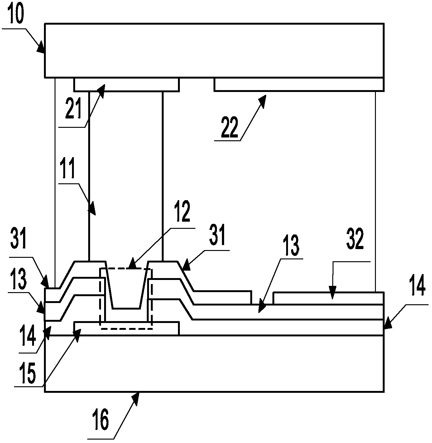
[0018] The invention provides a liquid crystal display panel, such as figure 1 As shown, the liquid crystal display panel includes: a color filter substrate 10 and an array substrate 16 after boxing; a layer structure for driving liquid crystal rotation is formed on the two substrates; the layer structure includes: a gate metal layer, a pixel electrode layer and Common electrode layer; wherein, the gate metal layer includes: PLG wiring 15; the common electrode layer includes: a first auxiliary electrode 21 and a common electrode 22, and there is no gap between the first auxiliary electrode 21 and the common electrode 22 Electrical connection; the first auxiliary electrode 21 is electrically connected to the PLG wiring 15 .

[0019] Wherein, the first auxiliary electrode 21 is electrically connected to the PLG wiring 15, that is, the resistance of the PLG wiring 15 is connected in parallel with the first auxiliary electrode 21 in the circuit, which can effectively reduce the re...

Embodiment 2

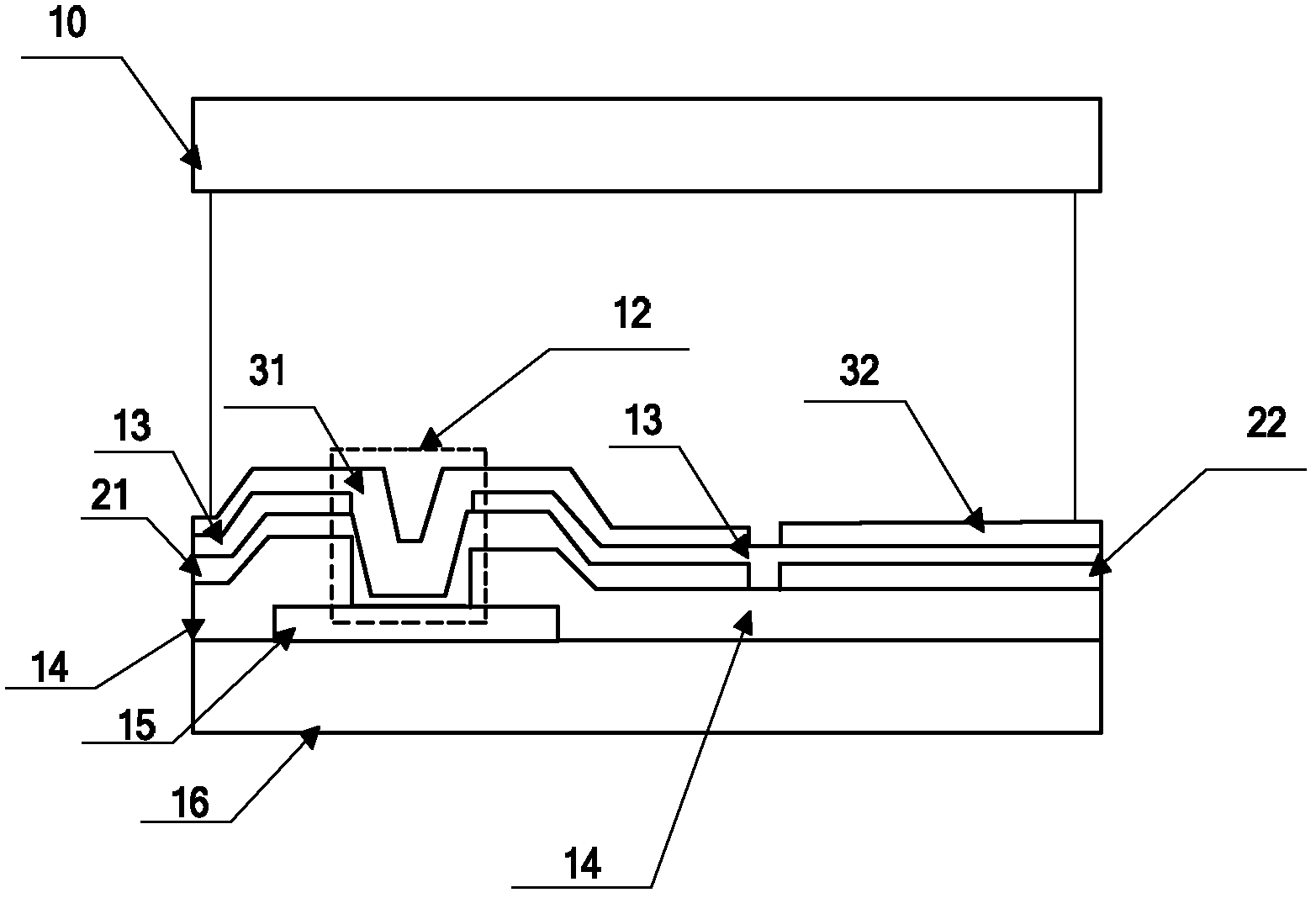
[0032] The invention provides a liquid crystal display panel, such as figure 2 As shown, the liquid crystal display panel includes: a color filter substrate 10 and an array substrate 16 after boxing; a layer structure for driving liquid crystal rotation is formed on the two substrates; the layer structure includes: a gate metal layer, a pixel electrode layer and Common electrode layer; wherein, the gate metal layer includes: connecting the gate PLG wiring 15; the common electrode layer includes: a first auxiliary electrode 21 and a common electrode 22, and the first auxiliary electrode 21 and the common electrode 22 There is no electrical connection between them; the first auxiliary electrode 21 is electrically connected to the PLG wiring 15 .

[0033] Further, at figure 2In the shown liquid crystal display panel, both the common electrode layer and the pixel electrode layer are formed on the array substrate 16, and the common electrode layer is below the pixel electrode la...

Embodiment 3

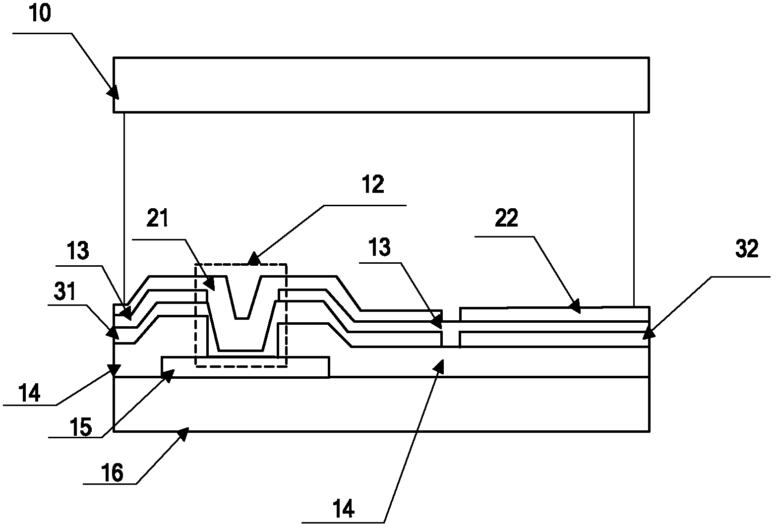
[0049] The invention provides a liquid crystal display panel, such as image 3 As shown, the liquid crystal display panel includes: a color filter substrate 10 and an array substrate 16 after boxing; a layer structure for driving liquid crystal rotation is formed on the two substrates; the layer structure includes: a gate metal layer, a pixel electrode layer and Common electrode layer; wherein, the gate metal layer includes: connecting the gate PLG wiring 15; the common electrode layer includes: a first auxiliary electrode 21 and a common electrode 22, and the first auxiliary electrode 21 and the common electrode 22 There is no electrical connection between them; the first auxiliary electrode 21 is electrically connected to the PLG wiring 15 .

[0050] Further, at image 3 In the shown liquid crystal display panel, both the common electrode layer and the pixel electrode layer are formed on the array substrate 16, and the pixel electrode layer is below the common electrode lay...


PUM


Abstract

The invention discloses a liquid crystal display panel and a liquid crystal display, relates to the field of liquid crystal panel manufacturing and is used for realizing the purposes of reducing the design complexity of PLG (Propel Link Gate) wiring and improving the manufacturing process precision. The liquid crystal display panel comprises a color film base plate and an array base plate which are subjected to box paring; layer structures for driving liquid crystal to rotate are formed on the two base plates; each layer structure comprises a gate metal layer, a pixel electrode layer and a common electrode layer, wherein the gate metal layer comprises a PLG wire; the common electrode layer comprises a first auxiliary electrode and a common electrode which are connected with each other in a non-electricity manner; and the first auxiliary electrode is electrically connected with the PLC wire. The scheme provided by the invention is suitable for the production and manufacturing of the liquid crystal display panel and the liquid crystal display.

Description

technical field [0001] The invention relates to the field of liquid crystal panel manufacturing, in particular to a liquid crystal display panel and a liquid crystal display. Background technique [0002] In the traditional process, the PLG (Propel Link Gate, connecting gate) wiring in the liquid crystal display panel is mainly used to transfer the signal output from the source IC (integrated circuit) to the gate IC, or to connect at least two gate ICs. Signals are transmitted between pole ICs. Usually, the PLG wiring is arranged on the edge of the liquid crystal display panel, and is fabricated on the same layer as the gate line and the bottom electrode line of the storage capacitor. The manufacturing process is as follows: a gate metal thin film is fabricated on the array substrate, and gate lines, storage capacitor electrodes and PLG wiring are formed through a patterning process. [0003] In the process of designing and making the above-mentioned PLG routing, the inven...

Claims


Application Information

Patent Timeline
IPC IPC(8): G02F1/1343G02F1/1345
CPCG02F1/136286G02F2201/121G02F1/1345G02F1/134318G02F1/134372G02F1/13629G02F1/134309
Inventor 王世君陈小川
Owner BOE TECH GRP CO LTD
Why Eureka
Try Eureka