Thin-film transistor (TFT) array substrate and display device
An array substrate and single-layer technology, which is applied in the field of TFT array substrates and display devices, can solve the problems of low on-current, low carrier mobility, and reduced switching characteristics of thin film transistors.
- Summary
- Abstract
- Description
- Claims
- Application Information
AI Technical Summary
Problems solved by technology
Method used
Image


Examples
Embodiment Construction
[0016] The following will clearly and completely describe the technical solutions in the embodiments of the present invention with reference to the accompanying drawings in the embodiments of the present invention. Obviously, the described embodiments are only some, not all, embodiments of the present invention. Based on the embodiments of the present invention, all other embodiments obtained by persons of ordinary skill in the art without making creative efforts belong to the protection scope of the present invention.
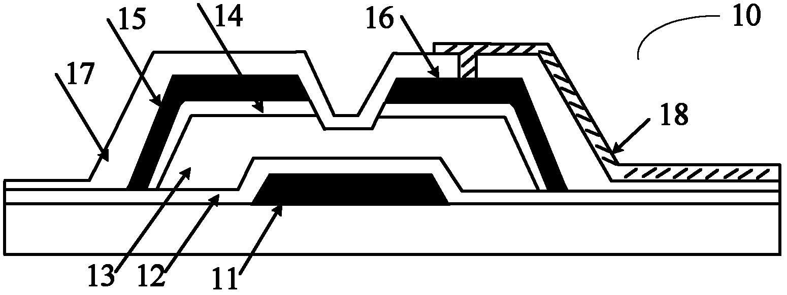
[0017] Such as figure 2 As shown, the embodiment of the present invention provides a TFT array substrate 20, including: data lines and gate lines, and thin film transistors formed in pixel units defined by the data lines and gate lines, and the thin film transistors include: gate 11. Gate insulating layer 12, active layer 13, ohmic contact layer 14, source electrode 15, and drain electrode 16; the active layer 13 is a superlattice structure, and the superlatt...
PUM
 Abstract
Description
Claims
Application Information
 - R&D
- Intellectual Property
- Life Sciences
- Materials
- Tech Scout
- Unparalleled Data Quality
- Higher Quality Content
- 60% Fewer Hallucinations
Browse by: Latest US Patents, China's latest patents, Technical Efficacy Thesaurus, Application Domain, Technology Topic, Popular Technical Reports.
© 2025 PatSnap. All rights reserved.Legal|Privacy policy|Modern Slavery Act Transparency Statement|Sitemap|About US| Contact US: help@patsnap.com