Light emitting diode packaging structure

A light-emitting diode and packaging structure technology, which is applied in the direction of electrical components, circuits, semiconductor devices, etc., can solve the problems of high target cost, inability to separate the base material, thin inside and thick outside, etc., and achieve the effect of uniform color temperature of light output

Inactive Publication Date: 2012-08-29
UNITY OPTO TECH CO LTD
View PDF3 Cites 8 Cited by
  • Summary
  • Abstract
  • Description
  • Claims
  • Application Information

AI Technical Summary

Problems solved by technology

[0009] 1: Although the spin-coating method can reduce the thickness of the phosphor layer, it has the phenomenon of thin inside and thick outside, and due to the influence between the phosphor layers, it cannot be separated from the substrate
[0010] 2: Although the process method of sputtering coating can achieve the effect of uniform dispersion of the phosphor layer, the cost of the target material is too high, resulting in high manufacturing costs, making it difficult to compete
[0011] 3: Although the ㄇ-shaped coating process can make the thickness of the phosphor layer consistent, it cannot reduce the serious phenomenon of phosphor deposition

Method used


Image

  • Light emitting diode packaging structure
  • Light emitting diode packaging structure
  • Light emitting diode packaging structure

Examples


Embodiment Construction

[0033] In order to enable your examiner to clearly understand the content of the invention, the following descriptions are provided with drawings, please refer to them.

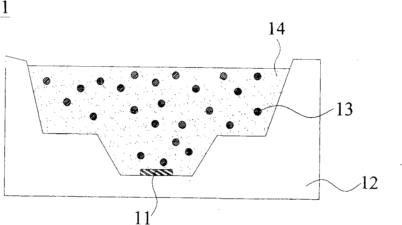
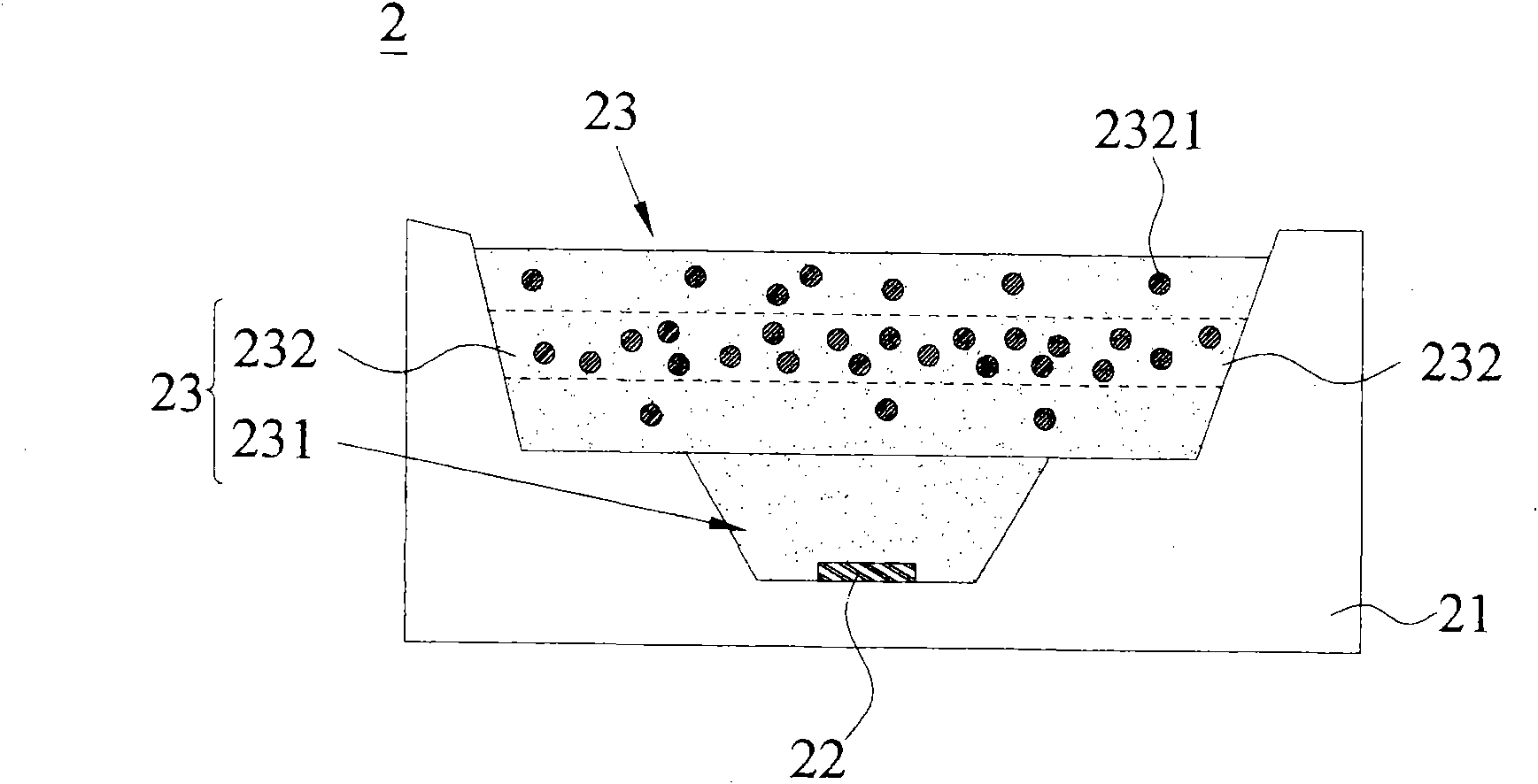
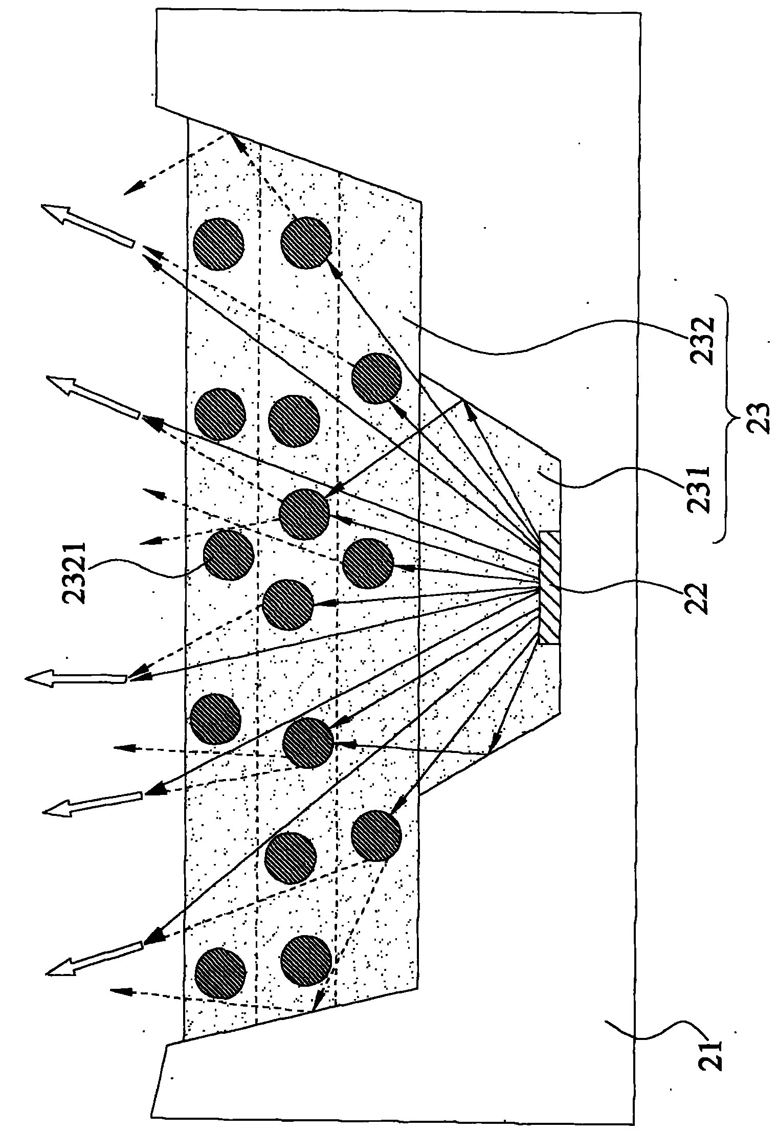
[0034] see figure 2 As shown, it is a schematic diagram of the first embodiment of the LED packaging structure of the invention. In the figure, the LED package structure 2 includes a base 21 , a LED chip 22 and a packaging compound 23 .

[0035] In this embodiment, the base 21 is an LED reflective cup. The light emitting diode chip 22 is a blue light emitting diode, which can emit a wavelength of about 450-460 nm after being driven, and is arranged on the bottom side of the base 21 . The encapsulant 23 includes a first optical adhesive 231 and a second optical adhesive 232 . The first optical adhesive material 231 can be epoxy resin (Epoxy) or silicone resin, and is coated on the LED chip 22 . The second optical adhesive material 232 can be epoxy resin (Epoxy) or silicone resin, and is disposed on one si...


PUM


Abstract

A light emitting diode (LED) packaging structure comprises a base, a LED chip and a packaging colloid. The LED chip is disposed in the base. The packaging colloid comprises a first optical resin material and at least one second optical resin material. The first optical resin material is transparent and packages the LED chip. The second optical resin material is disposed to a side of the first optical resin material. The second optical resin material is doped with a second fluorescent-powder. By disposing multilayered second optical resin materials, the fluorescent-powder is far from the LED chip to prevent the fluorescent-powder from being heated to cause light attenuation, thereby extending the service life of the LED chip.

Description

technical field [0001] The invention relates to a light emitting diode structure, in particular to a light emitting diode packaging structure. Background technique [0002] Light Emitting Diodes (LED) is a light source system made of solid materials such as semiconductors, which is different from traditional light sources such as incandescent lamps or various gas discharge lamps that must be operated in a vacuum or filled with a small amount of special gas . Compared with traditional light sources, white light-emitting diode light sources have many advantages, such as low power consumption, small size, fast response, high efficiency, environmental protection, and flat packaging. In terms of energy saving, its available life is as long as 60 years, which is 100 times that of traditional light bulbs, and the energy consumed is only 10% of traditional light bulbs. [0003] Since the successful development of high-power and high-brightness light-emitting diodes, the luminous e...

Claims


Application Information

Patent Timeline
Patent Type & Authority Applications(China)
IPC IPC(8): H01L33/48H01L33/56H01L33/50
CPCH01L33/504H01L33/507
Inventor 张暐路洹瀛沈士超
Owner UNITY OPTO TECH CO LTD
Why Eureka
Try Eureka