Treatment method and etching method of crystalline silicon wafer with oil stains

A technology of crystalline silicon wafer and processing method, applied in the field of texturing, can solve problems such as color spots of crystalline silicon wafer, and achieve the effect of improving the quality of finished products

Inactive Publication Date: 2012-09-05
WUXI SUNTECH POWER CO LTD +1
View PDF8 Cites 9 Cited by
  • Summary
  • Abstract
  • Description
  • Claims
  • Application Information

AI Technical Summary

Problems solved by technology

[0007] The technical problem to be solved by the present invention is to avoid undesirable phenomena suc

Method used


Image

  • Treatment method and etching method of crystalline silicon wafer with oil stains
  • Treatment method and etching method of crystalline silicon wafer with oil stains
  • Treatment method and etching method of crystalline silicon wafer with oil stains

Examples


Example Embodiment

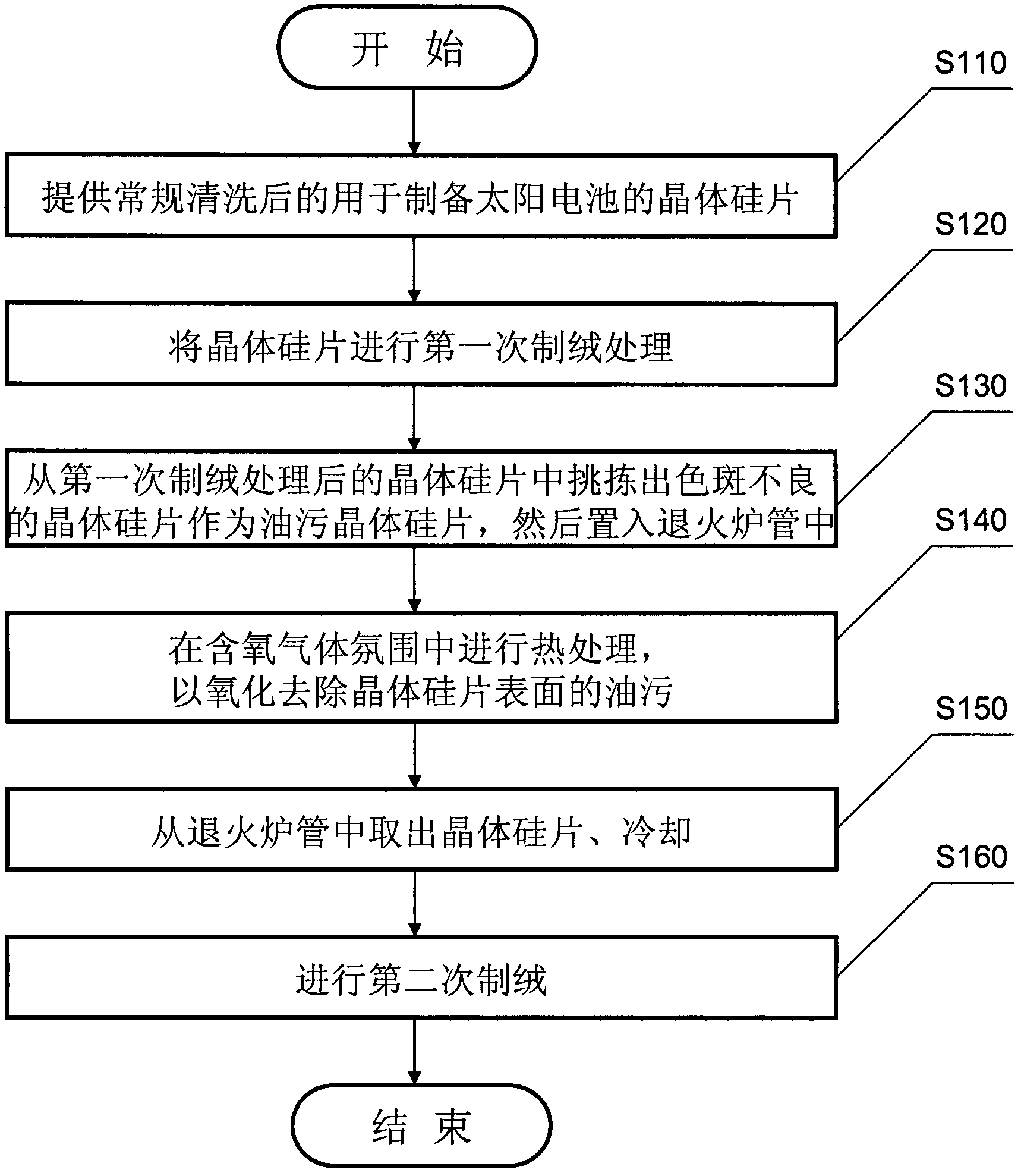
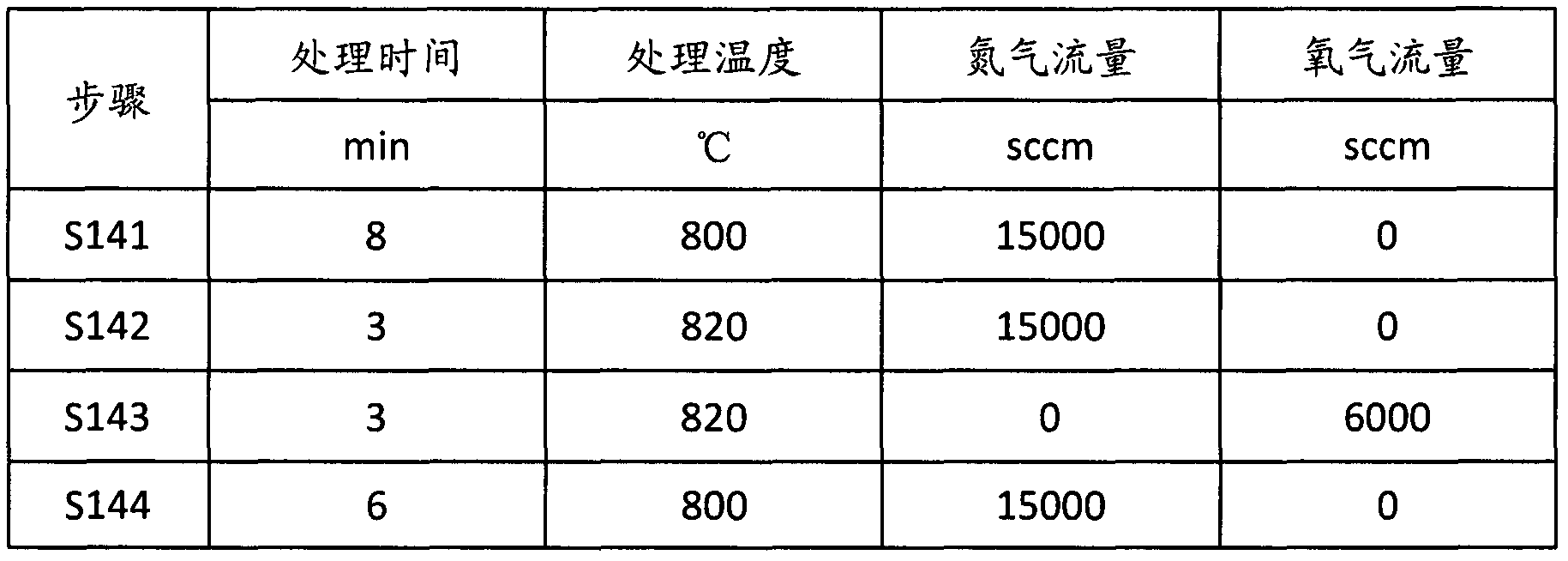
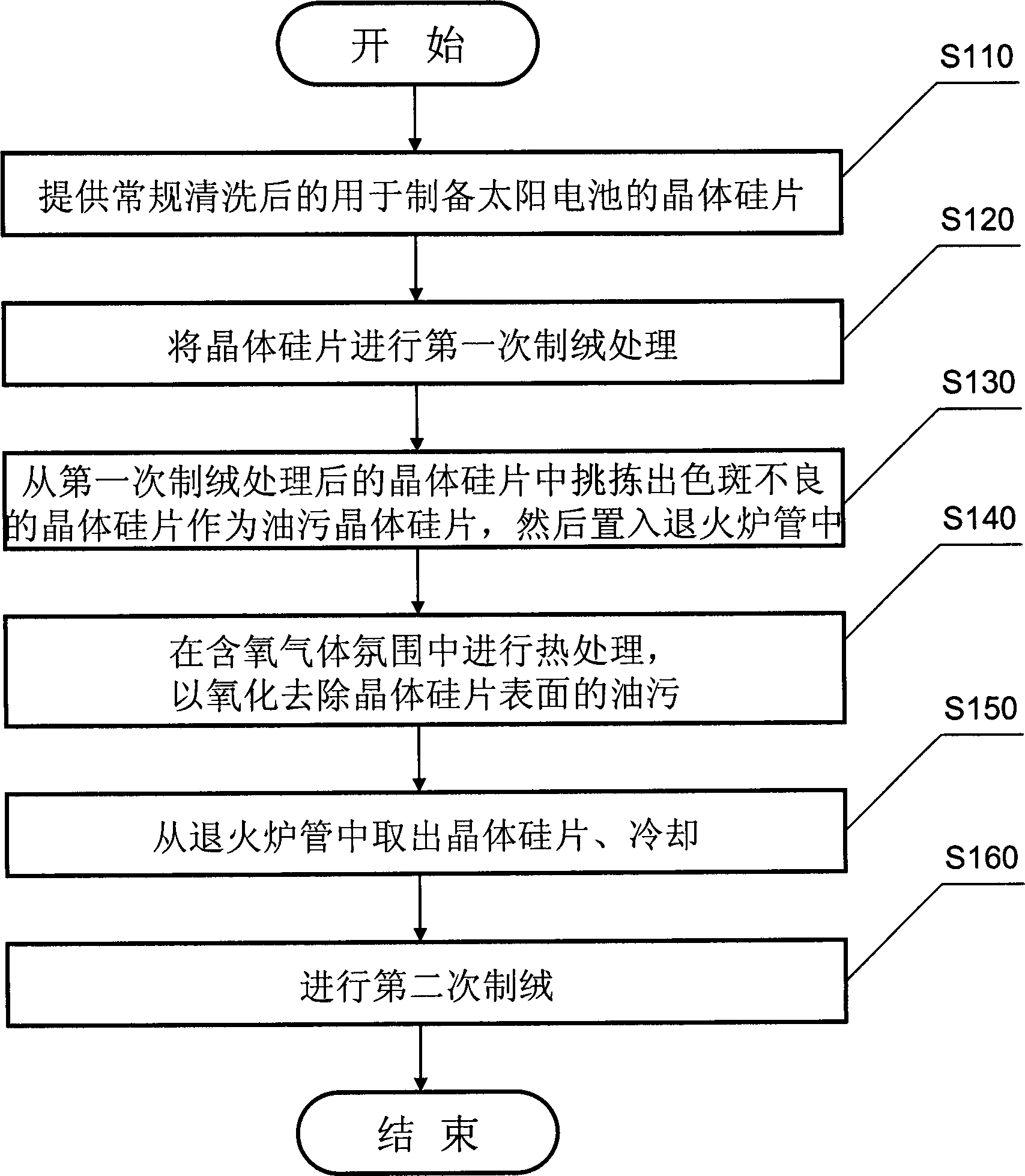
[0026] The following introduces some of the multiple possible embodiments of the present invention, which are intended to provide a basic understanding of the present invention, and are not intended to confirm the key or decisive elements of the present invention or limit the scope of protection. It is easy to understand that, according to the technical solution of the present invention, without changing the essential spirit of the present invention, those of ordinary skill in the art can propose other alternative implementation manners. Therefore, the following specific embodiments and drawings are only exemplary descriptions of the technical solutions of the present invention, and should not be regarded as all of the present invention or as a limitation or limitation to the technical solutions of the present invention.

[0027] figure 1 Shown is a schematic flow chart of a method for making texturing of solar cells according to an embodiment of the present invention. In this e...


PUM


Abstract

The invention provides a treatment method and an etching method of a crystalline silicon wafer with oil stains, belonging to the technical field of solar cell manufacturing. In the oil stain treatment method, the crystalline silicon wafer is subjected to heat treatment in an oxygen-containing gas atmosphere to remove the oil stains by oxidation. The etching method comprises the following steps: removing the oil stains on the crystalline silicon wafer with oil stains by oxidation after the primary etching, and carrying out secondary etching. The treatment method can effectively remove oil stains on the crystalline silicon wafer surface; and in the etching method using the treatment method, after the crystalline silicon wafer subjected to oil stain removal by oxidation is subjected to secondary etching, the crystalline silicon wafer subjected to the secondary etching can not have the phenomenon of defective color spots, thereby enhancing the quality of the etching finished product.

Description

technical field [0001] The invention belongs to the technical field of solar cell manufacturing, and relates to a treatment method for oily crystalline silicon wafers and a texturing method using the treatment method. Background technique [0002] Due to the limited supply of conventional energy and the increase in environmental protection pressure, many countries in the world have set off an upsurge in the development and utilization of solar energy and renewable energy, and solar energy utilization technology has developed rapidly. The use of electric energy is becoming more and more extensive. The crystalline silicon solar cell is one of the most commonly used devices to convert solar energy into electrical energy. [0003] In the preparation process of crystalline silicon solar cells, the following steps are mainly included: (1) removing the damaged layer, making texture and cleaning; (2) diffusing to prepare PN junction; (3) etching and removing edges; (4) cleaning pro...

Claims


Application Information

Patent Timeline
IPC IPC(8): C30B33/02C30B33/08
Inventor 刘娜何悦柳杉荣道兰
Owner WUXI SUNTECH POWER CO LTD
Why Eureka
Try Eureka