
Built-in self test and built-in self-repairing technology of TSV (Through Silicon Via) interconnection of 3D chip

A built-in self-test and built-in self-repair technology, applied in the field of built-in self-test and built-in self-repair technology, can solve problems such as the accuracy of the RC model that needs to be demonstrated, so as to reduce dependence, strengthen flexibility, and improve finished products rate effect

Inactive Publication Date: 2012-09-05
PEKING UNIV
View PDF6 Cites 22 Cited by
  • Summary
  • Abstract
  • Description
  • Claims
  • Application Information

AI Technical Summary

Problems solved by technology

Hung-Yen Huang et al. proposed a built-in self-test and built-in self-repair scheme for TSV interconnection. It is a simulation test technology by equating TSV to an RC model for charge and discharge testing, but the RC model of TSV The accuracy of the

Method used


Image

  • Built-in self test and built-in self-repairing technology of TSV (Through Silicon Via) interconnection of 3D chip
  • Built-in self test and built-in self-repairing technology of TSV (Through Silicon Via) interconnection of 3D chip
  • Built-in self test and built-in self-repairing technology of TSV (Through Silicon Via) interconnection of 3D chip

Examples


Embodiment Construction

[0017] The built-in self-test and built-in self-repair technology of 3D chip TSV interconnection provided by the present invention will be described in detail below with reference to the accompanying drawings.

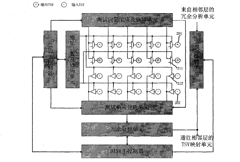
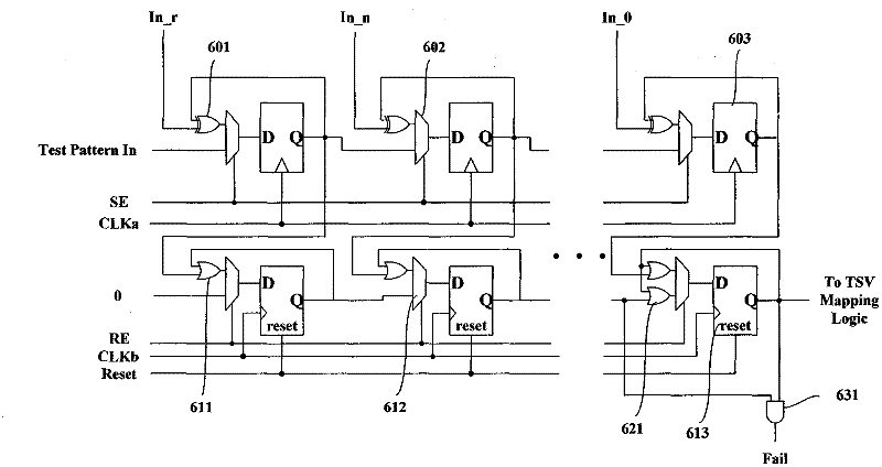
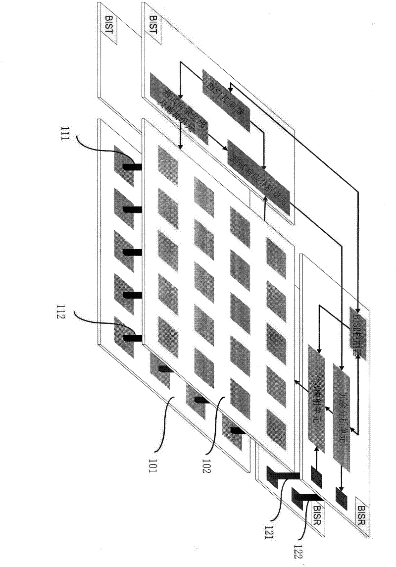
[0018] The technology mainly includes two parts, TSV built-in self-test circuit (BIST) and TSV built-in self-repair circuit (BISR). The BIST part includes the following parts: BIST controller, test vector generation and sending unit, address counting and decoding unit, test response analysis unit; BISR includes the following parts: BISR controller, TSV mapping unit, TSV redundancy analysis unit . The following describes the design and implementation of the main modules in conjunction with the accompanying drawings:

[0019] 1. The BIST main controller is used to control the work of other modules in the BIST circuit, and its state transition diagram is as follows Figure 4shown. After receiving the power-on reset signal (Power on Reset), the controller enters the INI...


PUM


Abstract

The invention relates to a built-in self test and built-in self-repairing technology of TSV (Through Silicon Via) interconnection of a 3D chip. The technology comprises the following steps: at the chip-designing stage, corresponding built-in self test and built-in self-repairing circuits are inserted, and a redundant TSV channel is designed; after power-on reset of the 3D chip, the built-in self test circuit starts to work, carries out grouped test on TSVs, generates corresponding TSV configuration information according to a test result, and then calls the built-in self-repairing circuit for configuration of a TSV mapping circuit, and simultaneously, the test of next group of TSVs is started; after the test and the configuration on all the TSVs, the circuits can enter normal working. The technology has the advantages that the difficulty of the TSV interconnection in the traditional 3D chip can be solved, the strategy can be replaced by redundancy, and the finished-product rate of the 3D chip is increased; the dependency of the 3D chip test on ATE (Automatic Test Equipment) is reduced, so that the test cost of the 3D chip is reduced; and due to independency from the specific chip function, the technology can be widely applied to the 3D chip based on the TSVs and has stronger practicability.

Description

technical field [0001] The invention discloses a built-in self-test and built-in self-repair technology for 3D chip TSV (through-silicon via) interconnection. Specifically, after the 3D chip is powered on and reset (Power-on Reset), the built-in self-test circuit starts to work, conducts group tests on TSVs, generates corresponding TSV configuration information according to the test results, and then calls the built-in self-repair circuit to TSV is configured, and when all TSV tests and configurations are completed, the circuit can enter normal operation. Background technique [0002] With the reduction of device size and the increase of circuit scale, the problems of delay and power consumption caused by interconnect lines are becoming more and more serious. In fact, this has become the most important bottleneck restricting circuit performance. The 3D chip realizes the vertical interconnection of multi-layer silicon wafers through silicon via technology, which increases th...

Claims


Application Information

Patent Timeline
IPC IPC(8): H01L21/66G01R31/28
Inventor 冯建华谭晓慧
Owner PEKING UNIV
Learn More