Array substrate, manufacturing method and display device thereof

An array substrate and substrate technology, applied in semiconductor/solid-state device manufacturing, instruments, semiconductor devices, etc., can solve problems such as manufacturing process limitations, device performance degradation, organic semiconductor thin film damage, etc., to simplify process steps and increase contact area. , the effect of reducing the difficulty of production

Active Publication Date: 2012-09-05
BOE TECH GRP CO LTD
View PDF6 Cites 21 Cited by
  • Summary
  • Abstract
  • Description
  • Claims
  • Application Information

AI Technical Summary

Problems solved by technology

[0003] like figure 1 As shown, the gate 1 of the thin film transistor with the bottom-gate-bottom-contact configuration is prepared on the substrate 3, the gate 1 is above the gate insulating layer 4, and the source and drain electrodes 2 are between the gate insulating layer 4 and the semiconductor film 5 , the boundary of the source-drain electrodes 2 under this structure will affect the deposition of the semiconductor thin film 5, which will reduce the molecular arrangement of the semiconductor thin film 5, thereby affecting the transport of its carriers, reducing the performance of the device, and further affecting the array substrate. quality; such as figure 2 As shown, the gate 1 of the thin film transistor with the bottom-gate top-contact configuration is also prepared on the substrate 3, the gate 1 is above the gate insulating layer 4, and the semiconductor film 5 is prepared on the gate insulating layer 4. Metal electrodes are regrown on the semiconductor film 5 to form the source-drain electrodes 2. The manufacturing process of the source-drain electrodes 2 under this structure is greatly limited, and the preparation of the source-drain electrodes 2 will cause damage to the organic semiconductor films that have been arranged in an orderly manner. , generally can only be formed by thermal evaporation, which is difficult to produce
At the same time, the existing array substrates of thin-film transistors with a bottom-gate bottom-contact configuration and a bottom-gate top-contact configuration require multiple photolithographic masks during the preparation process, which is cumbersome and expensive to produce.

Method used


Image

  • Array substrate, manufacturing method and display device thereof
  • Array substrate, manufacturing method and display device thereof
  • Array substrate, manufacturing method and display device thereof

Examples


Embodiment 1

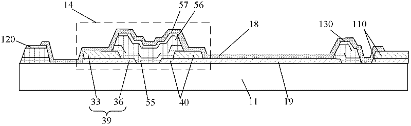
[0054] An embodiment of the present invention provides an array substrate, such as image 3 and Figure 4 As shown, the array substrate includes:

[0055] The substrate 11, and the gate lines 130, data lines 110, thin film transistors and pixel electrodes 19 located on the substrate, the thin film transistor is a thin film transistor 14 with a top-gate bottom-contact configuration, and the thin-film transistor with a top-gate bottom-contact configuration The gate of 14 (that is, the gate electrode pattern 57 ) is connected to the gate line 130 , the source 39 is connected to the data line 110 , and the drain 40 is connected to the pixel electrode 19 .

[0056] Further, the drain 40 of the thin film transistor is composed of upper and lower layers of electrodes, and the lower layer electrode and the pixel electrode 19 are integrally structured. This structure can realize better electrical contact between the drain electrode 40 and the pixel electrode 19 . Of course, the two ...

Embodiment 2

[0064] An embodiment of the present invention provides a method for manufacturing an array substrate, such as Figure 5 As shown, the method includes:

[0065] 101. Forming patterns including source and drain electrodes, pixel electrodes and data lines on the substrate through the first patterning process;

[0066] 102. Forming a pattern including a semiconductor layer, a gate insulating layer, a gate, and a gate line on the substrate that has completed the first patterning process through a second patterning process;

[0067] 103. Form a pattern including a passivation layer and passivation layer via holes on the substrate after the second patterning process through a third patterning process.

[0068] In the manufacturing method of the array substrate provided by the embodiment of the present invention, the source and drain electrodes of the thin film transistor with top-gate-bottom-contact configuration, the pixel electrodes and the data lines of the array substrate are fo...


PUM


Abstract

The invention provides an array substrate, a manufacturing method and a display device thereof, and relates to the technical field of display. The invention aims to reduce the production difficulty of the array substrate, simplify the manufacturing process of the array substrate and reduce the production cost. The array substrate comprises a thin-film transistor, wherein the thin-film transistor is formed by contact of a top grid positioned on a substrate; a grid electrode and a grid line of the thin-film transistor are connected, a source electrode is connected with a data line, and a drain electrode is connected with a pixel electrode. The manufacturing method of the array substrate comprises the following steps of: forming a graph including the source-drain electrodes, the pixel electrode and the data line on the substrate by a first-time composition process; forming a graph including a semiconductor layer, a grid-electrode insulating layer, the grid electrode and the grid line by a second-time composition process; and forming a graph including a passivation layer and passivation layer through holes by a third-time composition process. The display device comprises the array substrate.

Description

technical field [0001] The present invention relates to the field of display technology, in particular to an array substrate, a manufacturing method thereof, and a display device. Background technique [0002] Transistors are used as switching and driving devices to control and drive flat panel displays, such as liquid crystal displays, electroluminescent displays, and the like. Currently, thin film transistors of bottom-gate bottom-contact configuration and bottom-gate top-contact configuration are widely used in array substrates of liquid crystal displays. [0003] Such as figure 1 As shown, the gate 1 of the thin film transistor with the bottom-gate-bottom-contact configuration is prepared on the substrate 3, the gate 1 is above the gate insulating layer 4, and the source and drain electrodes 2 are between the gate insulating layer 4 and the semiconductor film 5 , the boundary of the source-drain electrodes 2 under this structure will affect the deposition of the semico...

Claims


Application Information

Patent Timeline
Patent Type & Authority Applications(China)
IPC IPC(8): H01L27/12H01L21/77H01L27/32
CPCH01L29/66757H01L27/1288G02F1/1368H01L29/7869G02F1/13685H10K10/84H10K10/82H10K10/464H10K19/10
Inventor 张学辉
Owner BOE TECH GRP CO LTD
Why Eureka
Try Eureka