Optimization method of SoC (System on Chip) address mapping

An optimization method and address technology, applied to instruments, electrical digital data processing, etc., can solve problems such as low efficiency of SoC address mapping, reduced circuit area, and reduced frequency of use of asynchronous FIFOs

Inactive Publication Date: 2012-09-12
SHANDONG SINOCHIP SEMICON
View PDF4 Cites 6 Cited by
  • Summary
  • Abstract
  • Description
  • Claims
  • Application Information

AI Technical Summary

Problems solved by technology

[0008] The present invention provides an optimized SoC address mapping method to overcome the low efficiency of the existing SoC address mapping method and the need to match a larger circuit area and more complex timing control, thereby reducing the frequency of use of asynchronous FIFOs , thereby reducing the area of ​​the circuit, and the overall timing control is relatively simple

Method used


Image

  • Optimization method of SoC (System on Chip) address mapping
  • Optimization method of SoC (System on Chip) address mapping
  • Optimization method of SoC (System on Chip) address mapping

Examples


Embodiment Construction

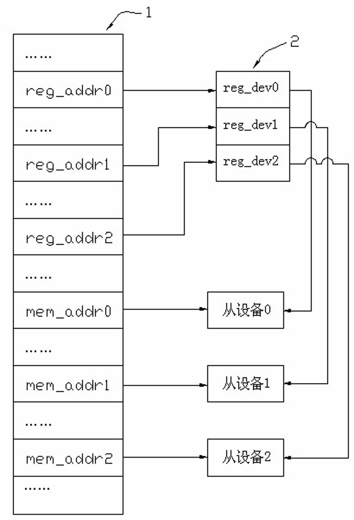
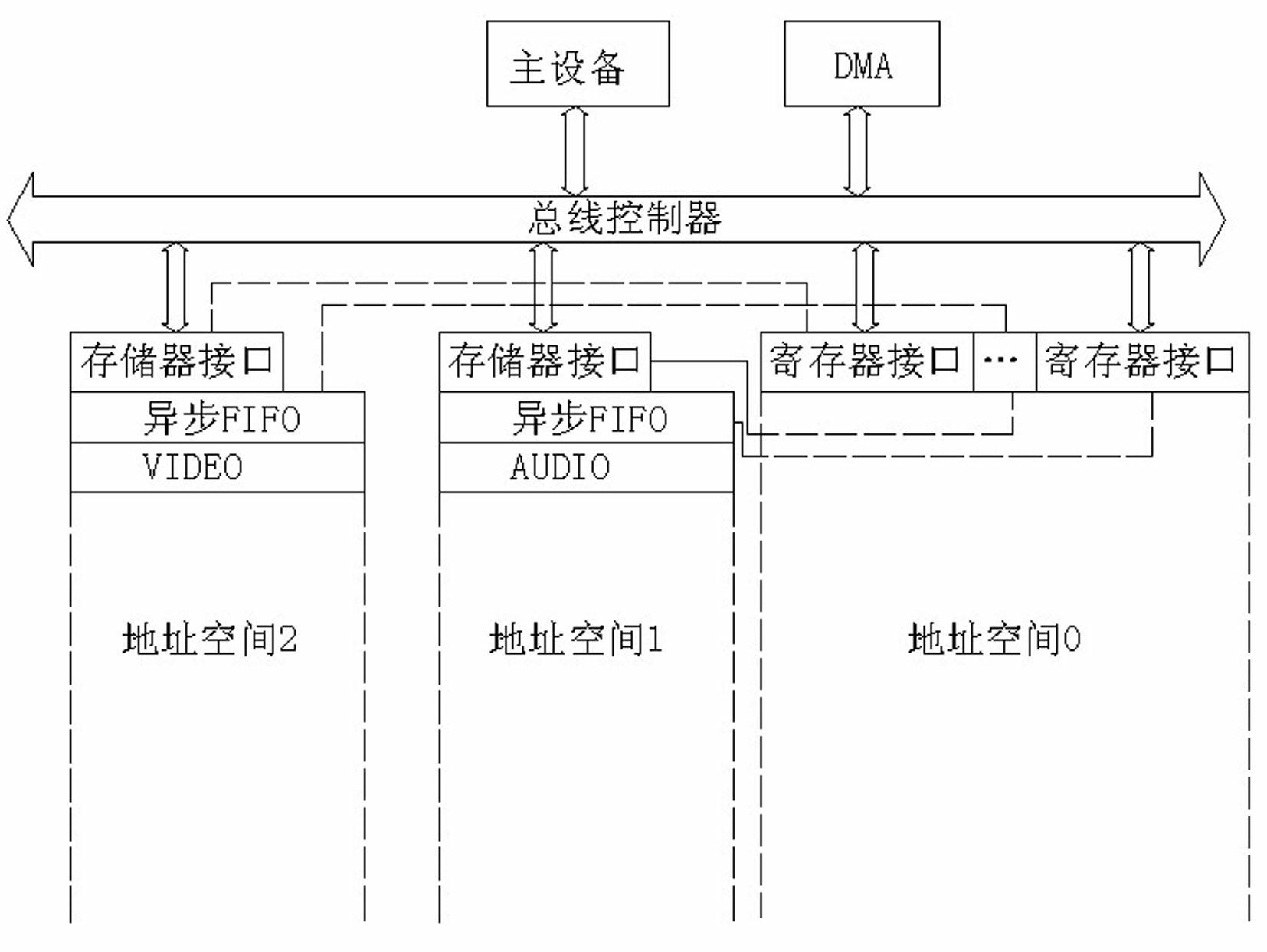
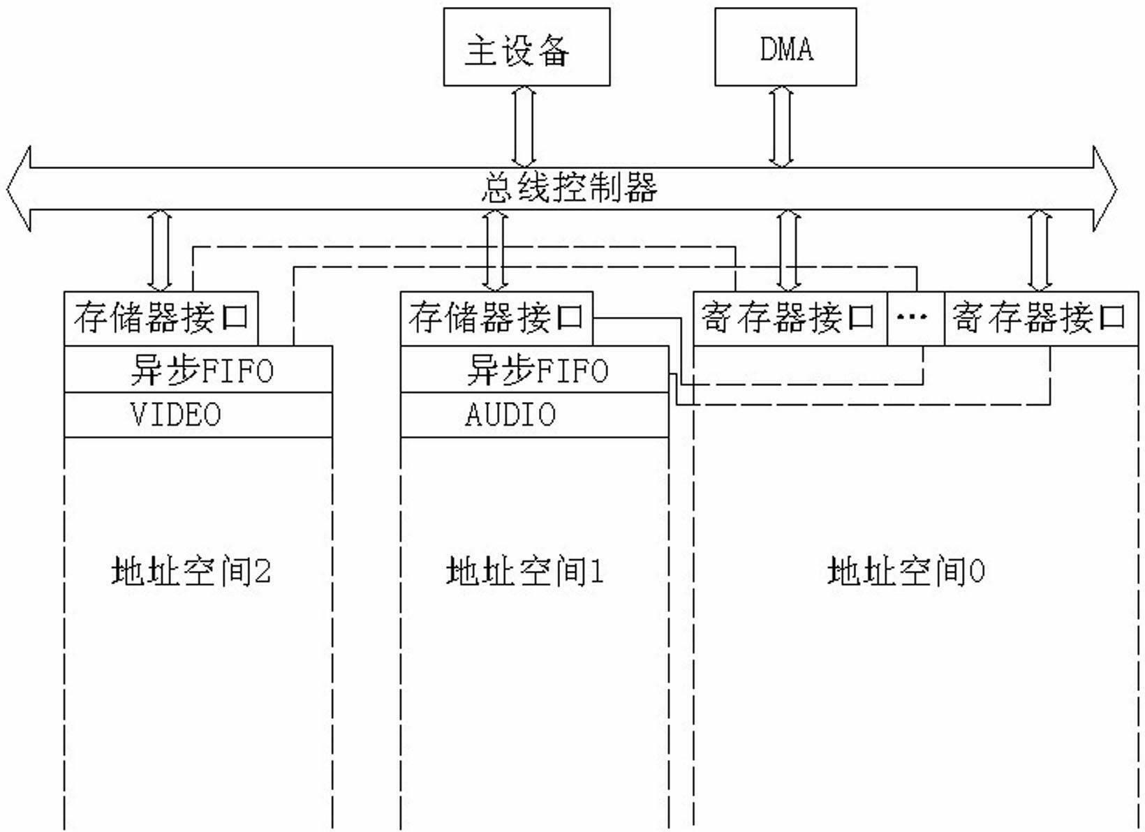
[0017] Refer to the attached figure 1 , the current common SoC address mapping method is that each slave device has an independent address port, combined with software, the hardware register group is allocated to another address space as a single device. In contrast, an embodiment according to the present invention presents figure 2 In this method, the existing address allocation method is maintained, that is to say, each slave device is mapped to two entry addresses, which are uniformly pushed into the CPU / DSP address stack, so that the CPU / DSP can find the corresponding function module. At the same time, the hardware Above, the register interface is implemented into the corresponding hardware module, and it is more accurately expressed as implemented into the memory interface. Under such configuration conditions, in terms of hardware architecture, it can be understood that each slave device corresponds to two address spaces.

[0018] Such as figure 2 As shown, the bus c...


PUM


Abstract

The invention discloses an optimization method of SoC (System on Chip) address mapping. The method comprises the steps that: an on-chip bus controller maps each slave into two entry addresses corresponding to a slave register interface and a memory interface, wherein the slave register interface entry address is overall assigned by a primary device and mapped to the address stack of the primary device; and at the same time the assigned slave register interface entry address is mapped into the corresponding slave by the bus controller. According to the invention, the use frequency of asynchronous FIFO (First Input First Output) is reduced, the circuit area is further reduced and the whole sequence control is relatively simple.

Description

technical field [0001] The invention relates to a method for organizing SoC (System on Chip, system on chip) IP (Intellectual Property) modules, in particular to a method for SoC address mapping. Background technique [0002] SoC is a system that integrates microprocessors, analog IP cores, digital IP cores, and memory (or off-chip memory interfaces) into a single chip, also called system-on-chip, and is a dedicated target integrated circuit. The typical structure of SoC usually consists of at least one high-performance CPU / DSP as the main controller or the main logic operation unit and several functional IPs connected through the on-chip bus. The CPU / DSP is called the main device or the main device, and the functional IP Known as a slave device or slave device. Therefore, the on-chip bus architecture, working mode, and working timing will greatly affect the operating efficiency of the SoC system and the operating efficiency of the SoC. [0003] In the current SoC bus syst...

Claims


Application Information

Patent Timeline
Patent Type & Authority Applications(China)
IPC IPC(8): G06F13/16G06F13/28
Inventor 孙晓宁张洪柳
Owner SHANDONG SINOCHIP SEMICON
Why Eureka
Try Eureka