Liquid crystal display device and manufacturing method thereof

A technology of a liquid crystal display device and a manufacturing method, applied in optics, instruments, nonlinear optics, etc., can solve problems such as limited array substrate yield, and achieve the effects of reducing energy consumption, improving success rate, and reducing waste

Active Publication Date: 2012-09-19
CHANGSHA HKC OPTOELECTRONICS CO LTD
View PDF7 Cites 11 Cited by
  • Summary
  • Abstract
  • Description
  • Claims
  • Application Information

AI Technical Summary

Problems solved by technology

[0005] The technical problem mainly solved by the present invention is to provide a liquid crystal display device and its manufacturing method to solve the problem in the prior art that the application of external voltage on the array substrate side is limited by the yield rate of the array substrate

Method used


Image

  • Liquid crystal display device and manufacturing method thereof
  • Liquid crystal display device and manufacturing method thereof
  • Liquid crystal display device and manufacturing method thereof

Examples


Embodiment Construction

[0030] The present invention will be described in detail below in conjunction with the accompanying drawings and embodiments.

[0031] The invention mainly proposes a liquid crystal display device in PSVA display mode and a manufacturing method thereof.

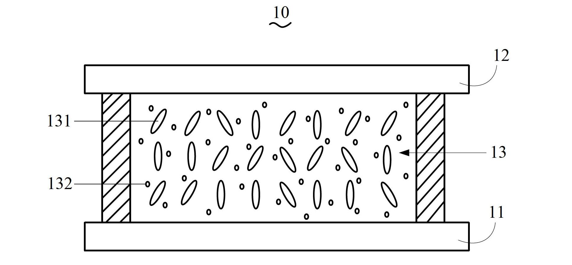
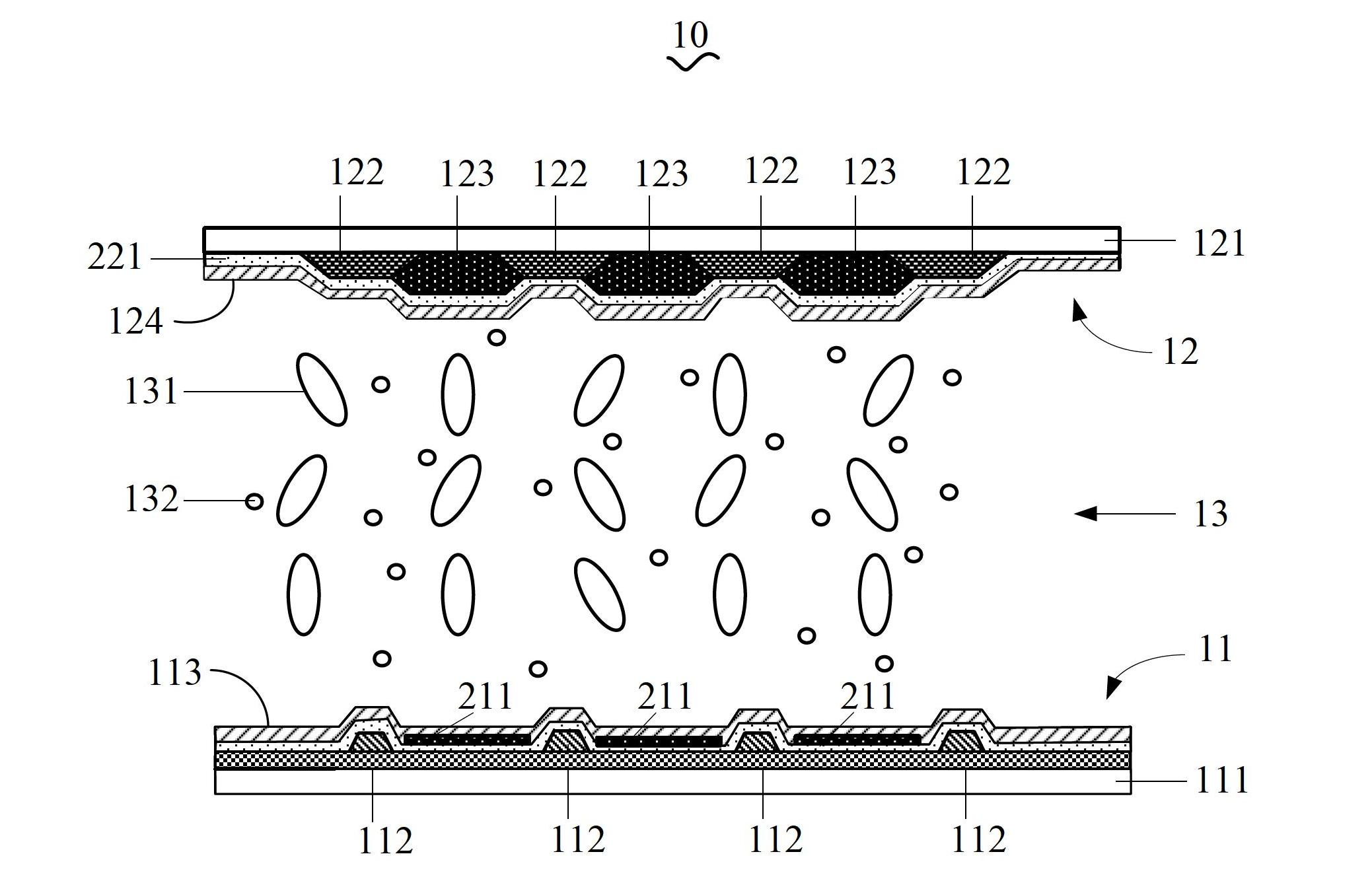
[0032] figure 1 It is a schematic structural view of the liquid crystal layer of the liquid crystal display device of the present invention before optical alignment. like figure 1 As shown, the liquid crystal display device 10 includes an array substrate 11 , a color filter substrate 12 opposite to each other, and a liquid crystal layer 13 filled between the two substrates.

[0033] The liquid crystal layer 13 is filled between the array substrate 11 and the color filter substrate 12 , and includes liquid crystal molecules 131 with negative dielectric anisotropy and reactive monomers 132 mixed in the liquid crystal molecules 131 . Wherein, the liquid crystal molecules 131 are liquid crystal materials that can be aligned in...


PUM


Abstract

The invention provides a liquid crystal display device and a manufacturing method thereof. The liquid crystal display device is provided with a plurality of pixel units. Each pixel unit comprises a liquid crystal layer, a pixel electrode and a counter electrode which are respectively arranged at two opposite sides of the liquid crystal layer, wherein the counter electrode comprises a first electrode pattern and a second electrode pattern, the first electrode pattern is arranged corresponding to the pixel electrode, and the second electrode pattern is connected with the first electrode pattern and used for applying an external voltage to the first electrode pattern, so that an alignment electric field of the liquid crystal layer is formed between the first electrode pattern and the pixel electrode. According to the liquid crystal display device and the manufacturing method thereof, the applying manner of the external voltage is changed, the external voltage is introduced from one side of a color filter substrate, the success ratio of liquid crystal alignment is increased, and thus, the energy consumption is decreased and the waste is reduced.

Description

technical field [0001] The invention relates to the field of liquid crystal display, in particular to a liquid crystal display device and a manufacturing method thereof. Background technique [0002] The current PSVA (Polymer Sustained Vertical Alignment, polymer stabilized vertical alignment technology) display mode liquid crystal display device mainly includes an array substrate (TFT substrate), a color filter substrate (CF substrate) opposite to each other, and filled in two liquid crystal layer between the substrates. Compared with liquid crystal display panels with wide viewing angle display modes such as MVA (Multi-Domain Vertical Alignment, multi-domain vertical alignment), PVA (Patterned Vertical Alignment, patterned vertical alignment), one of the advantages of PSVA display mode is color filtering There are neither protrusions nor ITO slits (Indium Tin Oxides Slit, indium tin oxide slits) on the sheet substrate. [0003] In the existing PSVA technology, in the Cel...

Claims


Application Information

Patent Timeline
Patent Type & Authority Applications(China)
IPC IPC(8): G02F1/1343G02F1/1333
CPCG02F1/1343G02F1/1337G02F1/133351G02F1/133711G02F1/1345G02F1/13775
Inventor 廖炳杰林家梁
Owner CHANGSHA HKC OPTOELECTRONICS CO LTD
Why Eureka
Try Eureka