Three-dimensional integrated method of sensor array and signal processing circuits

A signal processing circuit and sensor array technology, which is applied in the process of producing decorative surface effects, decorative arts, gaseous chemical plating, etc. The effect of large-scale array structure and simple manufacturing process

Inactive Publication Date: 2012-09-26
TSINGHUA UNIV
View PDF5 Cites 29 Cited by
  • Summary
  • Abstract
  • Description
  • Claims
  • Application Information

AI Technical Summary

Problems solved by technology

This method only provides the integration of the sensor and the signal processing circuit, and the suspension of the sensor's own structure still requires a separate process; at the same time, due to the influence of bonding, the process of the sensor structure suspension is generally arranged in the three-dimensional structure of the sensor and the signal processing circuit. After integration, a sensor structure with uniform thickness cannot be obtained

Method used


Image

  • Three-dimensional integrated method of sensor array and signal processing circuits
  • Three-dimensional integrated method of sensor array and signal processing circuits
  • Three-dimensional integrated method of sensor array and signal processing circuits

Examples


Embodiment Construction

[0064] The preferred embodiments will be described in detail below in conjunction with the accompanying drawings. It should be emphasized that the following description is only exemplary and not intended to limit the scope of the invention and its application.

[0065] A three-dimensional integration method of a sensor array and a signal processing circuit includes the following steps:

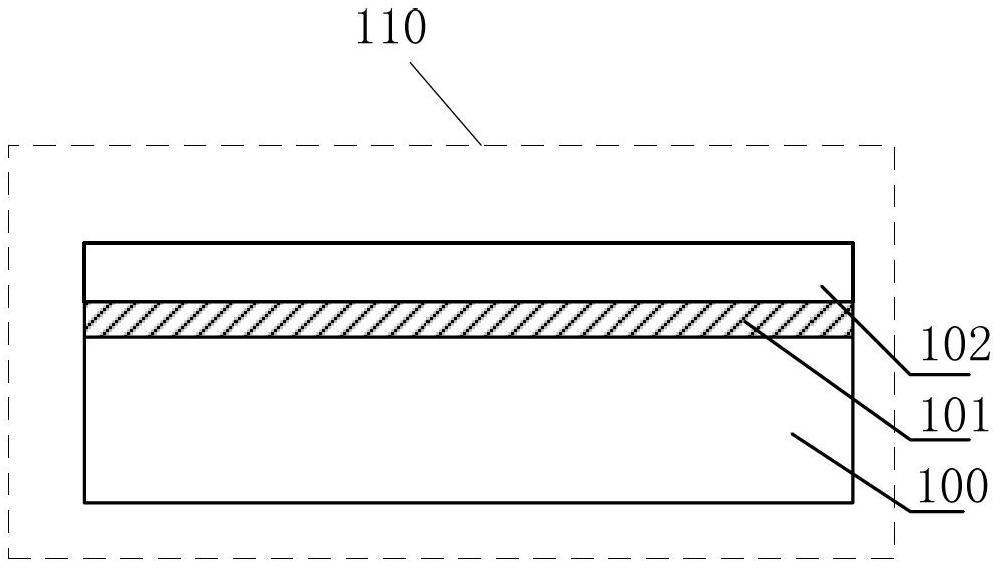
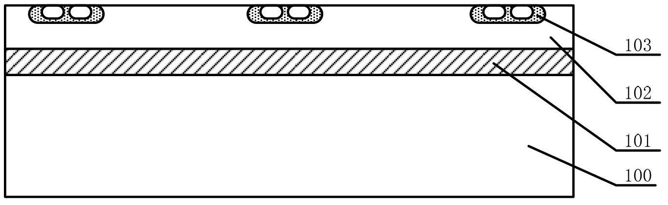
[0066] 1) if Figure 1a and Figure 1b As shown, the sensor 103 is fabricated on the top layer device layer material 102 of the insulating substrate device 110; the sensor structure can be fabricated at the initial stage, or can be manufactured after the top layer device layer material 102 is transferred to the signal processing circuit substrate 200, However, devices that require high-temperature processes, such as resistors, diodes, or transistors manufactured by implantation and annealing processes, need to be manufactured before bonding.

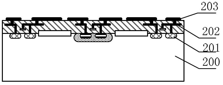
[0067] 2) Manufacturing a signal processing circ...


PUM


Abstract

The invention discloses a three-dimensional integrated method of a sensor array and signal processing circuits in the technical field of semiconductor three-dimensional integration. The three-dimensional integrated method comprises the following steps of: (1) manufacturing sensors on a top layer single crystal material of an insulating substrate device; (2) manufacturing the signal processing circuits and metal interconnection lines on the surface of a signal processing circuit substrate and manufacturing metal salient points on the metal interconnection lines; (3) carrying out a bonding process or a three-dimensional interconnection process; (4) carrying out metal thermocompression bonding on bonding metal salient points and the salient points; (5) removing a temporary bonding polymer layer and auxiliary wafers; and (6) manufacturing plane interconnection lines. By utilizing the three-dimensional integrated method, integration of the sensors and the signal processing circuits is realized, hovering of the sensors is realized, electric signal connection of the sensors and the signal processing circuits is realized by utilizing three-dimensional interconnection lines, the manufacture process is simple, the sensors can be suspended, and excellent consistency of the sensors and large-scale array structure can be obtained.

Description

technical field [0001] The invention belongs to the technical field of three-dimensional integration of semiconductors, in particular to a three-dimensional integration method of a sensor array and a signal processing circuit. Background technique [0002] The development of micro-electro-mechanical systems (MEMS) technology has greatly promoted the development of sensor technology. The miniaturization of sensors through MEMS technology can not only realize the sensitive mechanism that cannot be obtained by macroscopic devices, but also make full use of the excellent mechanical properties of silicon materials. Reducing the size, power consumption and cost of the sensor can also realize the array words and redundancy of the micro sensor, and can realize the monolithic integration of the sensor and the signal processing circuit. The monolithic integration of the sensor and the signal processing circuit makes the signal processing circuit close to the sensor itself, which can r...

Claims


Application Information

Patent Timeline
Patent Type & Authority Applications(China)
IPC IPC(8): B81C1/00
Inventor 王喆垚陈倩文宋振唐浩
Owner TSINGHUA UNIV
Why Eureka
Try Eureka