CMOS image sensor and exposure control method thereof

An image sensor and exposure control technology, applied in the field of image sensors, can solve problems affecting image quality and perception

Active Publication Date: 2012-09-26
BRIGATES MICROELECTRONICS KUNSHAN
View PDF4 Cites 24 Cited by
  • Summary
  • Abstract
  • Description
  • Claims
  • Application Information

AI Technical Summary

Problems solved by technology

However, when the indoor light is relatively strong and the exposure time is shorter than 10ms, yellow bands or oth

Method used


Image

  • CMOS image sensor and exposure control method thereof
  • CMOS image sensor and exposure control method thereof
  • CMOS image sensor and exposure control method thereof

Examples


Embodiment Construction

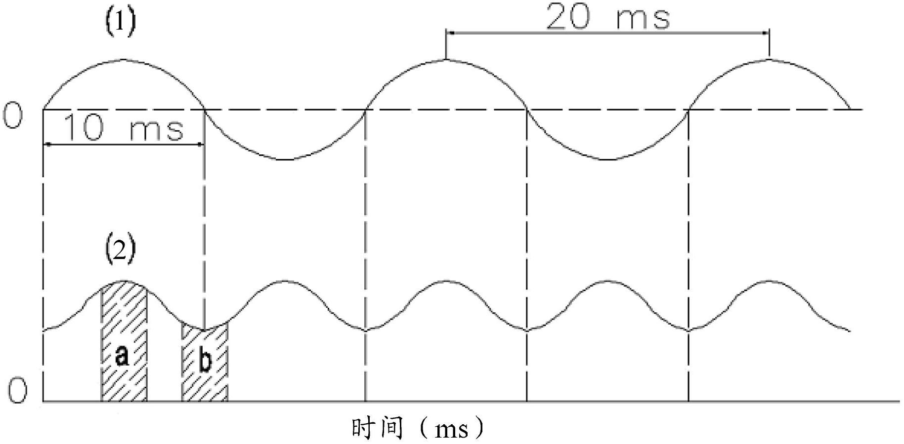
[0051] As mentioned in the background art, when the CMOS image sensor works under the condition of indoor fluorescent light, yellow bands or other alternate light and dark bands often appear on the image, which seriously affects the quality and perception of the image. The inventor has researched and analyzed the reason of this phenomenon.

[0052] Please refer to figure 2 , (1) represents the 50Hz mains power, and the light intensity change cycle is 20ms; (2) represents the light intensity change of the fluorescent lamp driven by the mains power, and its cycle is 10ms.

[0053] As mentioned in the background art, traditional CMOS image sensors generally adopt a row-by-row rolling exposure method, and the start time of each row of exposure is different, but the exposure time length of all rows is the same.

[0054] Assume that the exposure time is much less than 10ms under good light conditions. Such as figure 2 As shown in (2), it is assumed that the exposure time of a c...


PUM


Abstract

The invention discloses a CMOS (Complementary Metal Oxide Semiconductor) image sensor and an exposure control method thereof. The method comprises the following steps: aiming at a pixel array, first row-to-row exposure and second row-to-row exposure are executed to obtain first image data and second image data, the exposure time interval of the same row of the first row-to-row exposure and the second row-to-row exposure is longer than a half light intensity period of change by odd number times; and image data in the same row of the first image data and the second image data is compound to obtain an output image. The CMOS image sensor comprises an exposure time sequence control circuit, row selecting circuits, a pixel array, a reading circuit and an image compound circuit, wherein the row selecting circuit executes the first row-to-row exposure and the second row-to-row exposure for the pixel array, the exposure time interval of the same row of the first row-to-row exposure and the second row-to-row exposure is longer than a half light intensity period of change by odd number times, and the image compound circuit compounds the first image data and the second image data to form an output image. By adopting the CMOS image sensor and the exposure control method thereof, yellow bands or light and shade strips in an image are eliminated.

Description

technical field [0001] The invention relates to the technical field of image sensors, in particular to a CMOS image sensor and an exposure control method thereof. Background technique [0002] Image sensors are semiconductor devices that convert light signals into electrical signals. Currently, conventional image sensors include charge coupled device (CCD) image sensors and complementary metal oxide semiconductor (CMOS) image sensors. Since the CMOS image sensor has the advantages of low power consumption and high signal-to-noise ratio, it is widely used in the field of image sensors. [0003] The Chinese patent with the publication number CN101212580A discloses a typical CMOS image sensor with four-tube structure, and the pixel unit circuit diagram of the sensor is as follows: figure 1 shown. It mainly includes a photodetector PPD, a transmission tube T1, a reset tube T2, a source follower T3, and a selection tube T4. The photodetector PPD is a photodiode that generates...

Claims


Application Information

Patent Timeline
IPC IPC(8): H04N5/359H04N5/3745H04N5/378
Inventor 罗文哲
Owner BRIGATES MICROELECTRONICS KUNSHAN
Why Eureka
Try Eureka