Work structure for providing scanning path of immersion photoetching machine

A technology of scanning path and lithography machine, which is applied in the field of microelectronics and can solve problems such as low product yield

Inactive Publication Date: 2012-10-03
SHANGHAI HUALI MICROELECTRONICS CORP
View PDF0 Cites 3 Cited by
  • Summary
  • Abstract
  • Description
  • Claims
  • Application Information

AI Technical Summary

Problems solved by technology

[0004] like figure 1 as shown in figure 1 Including a silicon wafer 1, the silicon wafer includes a plurality of wafers (wafer) 2, the traditional scanning path structure is exposed from the top of the wafer in an "S" shape, but the working structure of the scanning path is due to premature

Method used


Image

  • Work structure for providing scanning path of immersion photoetching machine
  • Work structure for providing scanning path of immersion photoetching machine
  • Work structure for providing scanning path of immersion photoetching machine

Examples


Embodiment Construction

[0016] The present invention will be further described below in combination with the principle diagram and specific operation embodiments.

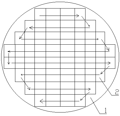
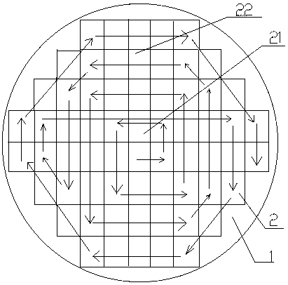
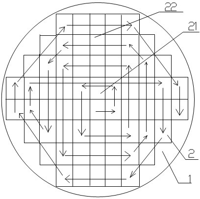
[0017] See figure 2 As shown in the present invention, a working structure for providing a scanning path of an immersion lithography machine specifically includes:

[0018] A silicon wafer 1, the silicon wafer includes a plurality of wafers 2, on the substrate surface of the silicon wafer 1 includes a bottom anti-reflective layer (not shown in the figure), photoresist (not shown in the figure); in order to prevent immersion The volatiles of the photoresist damage the lens of the lithography machine, and a top coating layer (not shown in the figure) may be included on the surface of the photoresist, which can be completely dissolved in the developing liquid Hydrophobic coating. The top coating layer can also be a layer of top anti-reflective coating (TARC), which is coated on the surface of the photoresist to reduce light reflection.

[0019]...


PUM


Abstract

The invention discloses a work structure for providing a scanning path of an immersion photoetching machine. The work structure comprises a silicon wafer which is arranged below an exposure lens of the immersion photoetching machine, and the work structure is characterized in that the silicon wafer comprises a plurality of wafers, and each of the plurality of wafers further comprises a bottom anti-reflection layer and a photo resist; and a plurality of wafers comprise the wafers in a central scanning path area and the wafers in a peripheral scanning path area, and the central scanning path area and the peripheral scanning path area are both in the spiral scanning path structures. According to the work structure provided by the invention, the wafers in the silicon wafer to be exposed are divided into two areas, and the two areas are both in the spiral scanning work path structures, in this way, most part of the silicon wafer is prevented from being impacted by the particles, and the exposure quality can be achieved and the yield of the product can be increased.

Description

Technical field [0001] The invention relates to the field of microelectronics, in particular to a working structure for providing a scanning path of an immersion lithography machine. Background technique [0002] With the rapid development of semiconductors, immersion lithography machines are uniformly adopted in the industry for 55nm processes and below. Because the immersion lithography machine uses pure water to improve the resolution during exposure, and when using pure water for exposure, more particles are introduced. The source is mainly the particles on the back of the silicon wafer at the edge of the wafer. [0003] This is because the source of particles during exposure is mainly introduced during exposure to the edge of the silicon wafer, and the particles introduced during exposure are mainly introduced when exposed to the edge of the silicon wafer (wafer edge), because pure water will diffuse to the back of the wafer; because usually the wafer The back side is the mai...

Claims


Application Information

Patent Timeline
IPC IPC(8): G03F7/20
Inventor 蔡恩静
Owner SHANGHAI HUALI MICROELECTRONICS CORP
Why Eureka
Try Eureka