Pixel unit circuit, working method therefore and organic light emitting diode (OLED) display device

A pixel unit and circuit technology, applied in static indicators, instruments, etc., can solve problems such as electrical performance non-uniformity, current difference, mura, etc., and achieve the effect of improving display effect and compensating for degradation

Active Publication Date: 2012-10-03
BOE TECH GRP CO LTD
View PDF6 Cites 24 Cited by
  • Summary
  • Abstract
  • Description
  • Claims
  • Application Information

AI Technical Summary

Problems solved by technology

Since the voltage of ARVDD is related to the current, IR Drop will also cause the current difference in different regions, and then produce the mura phenomenon when displaying;
[0006] Third, the uneven film thickness of OLED devices will also cause non-uniformity in electrical properties during evaporation.
It can be seen from the above formula that if the V between different pixel units th different, there is a difference in current
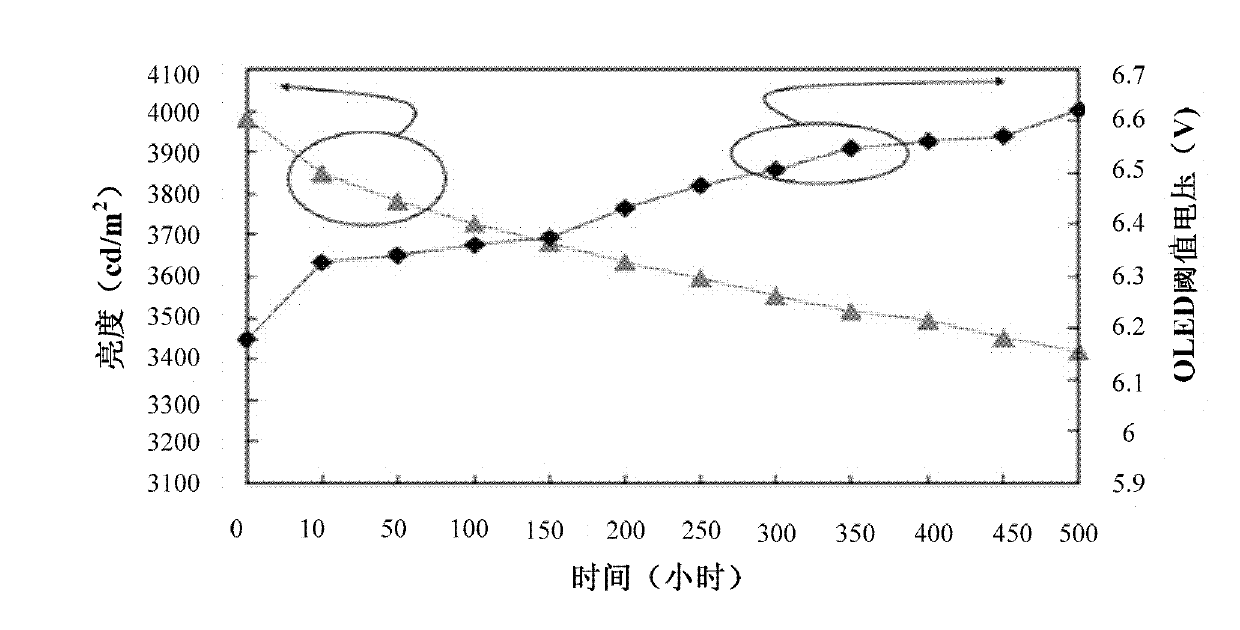
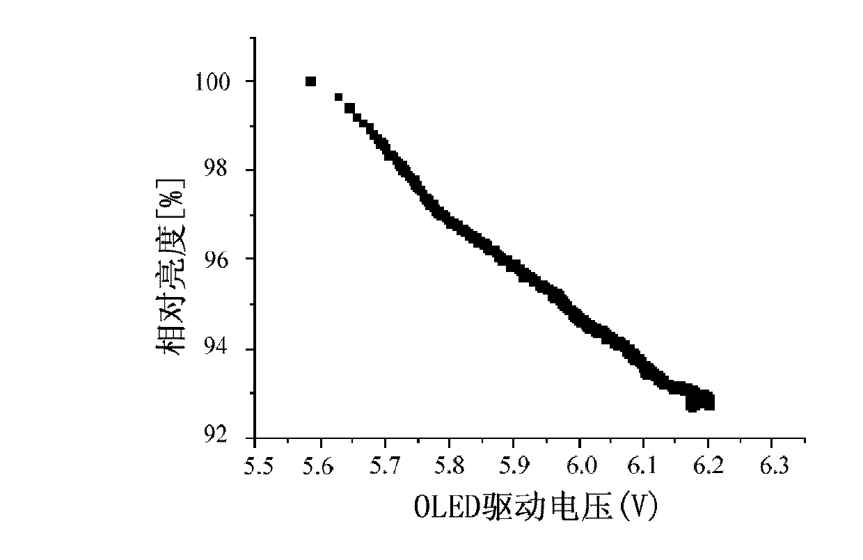
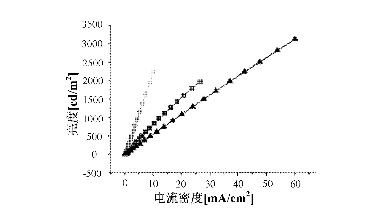
And as the OLED device degrades, even if a constant current is provided, the luminous brightness of the OLED will decrease
[0013] present, the compensation V th There are many types of pixel unit structures for uniformity and IR drop, but some pixel unit structures can compensate for the V of the drive tube th Non-uniformity, but it cannot compensate the brightness loss caused by IR Drop and

Method used


Image

  • Pixel unit circuit, working method therefore and organic light emitting diode (OLED) display device
  • Pixel unit circuit, working method therefore and organic light emitting diode (OLED) display device
  • Pixel unit circuit, working method therefore and organic light emitting diode (OLED) display device

Examples


Embodiment Construction

[0086] In general, the pixel unit circuit proposed by the present invention includes: a first sub-circuit module, a second sub-circuit module, a capacitor and an organic light-emitting display diode OLED; wherein,

[0087] An input end of the first sub-circuit module is connected to the data line;

[0088] The other input end of the first sub-circuit module is connected to the output end of the second sub-circuit module and the OLED;

[0089] The output end of the first sub-circuit module is connected to the input-output end of the second sub-circuit module through a capacitor;

[0090] The output end of the second sub-circuit module is connected to the OLED, and the voltage difference between the positive and negative power supplies of the backplane is applied to both ends.

[0091] Wherein, the first sub-circuit module is used to select the input voltage to output to the capacitor; the second sub-circuit module is used to convert the input voltage into current and provide i...


PUM


Abstract

The invention discloses a pixel unit circuit, which consists of a first sub-circuit module, a second sub-circuit module, a capacitor and an organic light emitting diode (OLED). The main working process of the pixel unit circuit is divided into a compensation stage and an evaluation stage. Compared with the traditional pixel unit circuit, the pixel unit circuit is characterized in that the degeneration of the OLED device, the threshold voltage heterogeneity of a thin film transistor (TFT) driving pipe and the IR drop of a rear panel power supply can be effectively compensated. In addition, because the pixel unit circuit provided by the invention is designed on the basis of the voltage feedback technology, the pixel unit circuit is suitable to apply to a big-size panel. In addition, the invention also correspondingly discloses a working method for the pixel unit circuit and an OLED display device comprising a plurality of pixel unit circuits connected in series.

Description

technical field [0001] The present invention relates to pixel circuit design technology, in particular to a pixel unit circuit and its working method, and an organic light-emitting diode (Organic Light-Emitting Diode, OLED) display device. Background technique [0002] OLED, as a current-mode light-emitting device, has been increasingly used in high-performance displays. With the increase of display size, traditional passive matrix organic light-emitting diode (Passive Matrix OLED, PMOLED) displays require shorter driving time of a single pixel, so it is necessary to increase the transient current and increase power consumption. At the same time, high-current The application will cause an excessive voltage drop on the indium tin oxide (ITO) line, and make the OLED operating voltage too high, thereby reducing the efficiency of the OLED, and the active matrix organic light-emitting diode (Active Matrix OLED, AMOLED) display through the progressive scan input of the switch tube...

Claims


Application Information

Patent Timeline
IPC IPC(8): G09G3/32
CPCG09G2320/045G09G2300/0852G09G2300/0861G09G2320/043G09G3/3233G09G2300/0819G09G3/30
Inventor 吴仲远段立业王刚肖田
Owner BOE TECH GRP CO LTD
Why Eureka
Try Eureka