Oxide film transistor and preparation method thereof, array substrate and display device

A technology of oxide film and manufacturing method, which is applied in the direction of transistor, semiconductor/solid-state device manufacturing, semiconductor device, etc., can solve the problems of active layer etching, affecting transistor performance, diffusion, etc., and achieve process simplification and good production yield , The effect of production yield control

Active Publication Date: 2015-06-10
BOE TECH GRP CO LTD
View PDF8 Cites 0 Cited by
  • Summary
  • Abstract
  • Description
  • Claims
  • Application Information

AI Technical Summary

Problems solved by technology

In the manufacturing process of the existing oxide thin film transistor, the drain electrode 105-1 and the source electrode 105-2 are patterned by wet etching. The active layer 103 also has an etching effect, so an etch barrier layer 104 is used to ensure that the active layer 103 is not etched when the source and drain metal layers are etched. The disadvantage of this process is that the H+ ions in the etch barrier layer will Diffusion into the active layer 103 affects the performance of the transistor, and the active layer is more or less etched
[0008] In another existing manufacturing method of an oxide thin film transistor, the active layer is arranged on the source electrode and the drain electrode. In order to form the active layer, an etch barrier layer is required to ensure that the active layer is etched to form an active layer. The source electrode and drain electrode are not etched when layering. The disadvantage of this process is that the H+ ions in the etch barrier layer will diffuse into the source electrode and drain electrode to affect the performance of the transistor, and more or less there will be source The phenomenon that the electrode and the drain electrode are etched

Method used


Image

  • Oxide film transistor and preparation method thereof, array substrate and display device
  • Oxide film transistor and preparation method thereof, array substrate and display device
  • Oxide film transistor and preparation method thereof, array substrate and display device

Examples


Embodiment Construction

[0039] The invention provides an oxide thin film transistor, a manufacturing method thereof, an array substrate and a display device. The oxide thin film transistor manufacturing method described in the present invention can be applied to oxide thin film transistors with top-gate top-contact, top-gate bottom-contact, bottom-gate, double-gate and other structures.

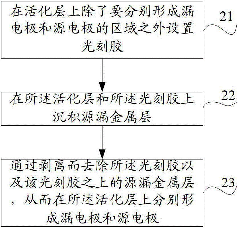
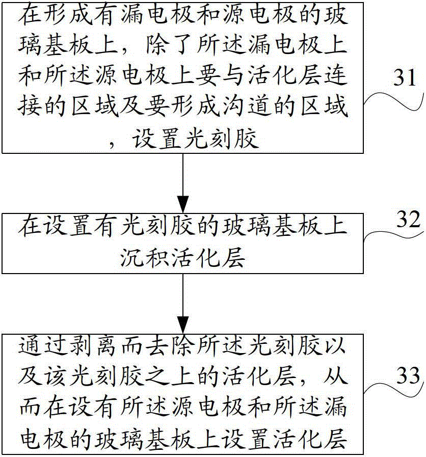
[0040] The manufacturing method of the oxide thin film transistor according to the present invention comprises the following steps: between forming the active layer and the passivation layer, at least setting a photoresist outside the area where the source electrode contacts the drain electrode and the active layer; then stripping the photoresist Engraving.

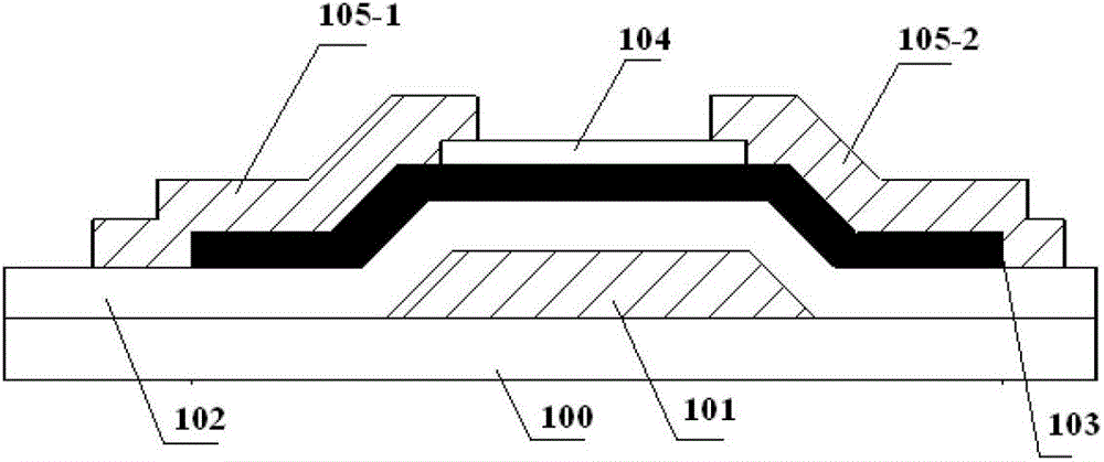
[0041] The oxide thin film transistor of the present invention includes a substrate, a source electrode, a drain electrode, an activation layer and a passivation layer;

[0042] The source electrode, the drain electrode, the activation layer and the passivatio...


PUM


Abstract

Provided are an oxide thin film transistor and manufacturing method thereof, array substrate and display device, the oxide thin film transistor comprising a substrate (100), a source electrode (104-2), a drain electrode (104-1), an activation layer (103), and a passivation layer (105); the source electrode, the drain electrode, the activation layer, and the passivation layer are disposed on the substrate; the source electrode and the drain electrode are provided with a grooved area therebetween; and the passivation layer directly contacts the activation layer at least in the groove area. By this, the present invention avoids the damage to the activation layer, or the drain electrode and the source electrode of the oxide thin film transistor caused by an etched barrier layer in the manufacturing process of the oxide thin film transistor.

Description

technical field [0001] The invention relates to the field of display, in particular to an oxide thin film transistor, a manufacturing method thereof, an array substrate and a display device. Background technique [0002] Organic light-emitting display devices are a new generation of display devices. Compared with liquid crystal displays, they have many advantages, such as: self-illumination, fast response speed, wide viewing angle, etc., and can be used for flexible display, transparent display, 3D display, etc. [0003] The active matrix light-emitting display is equipped with a switch-thin film transistor for controlling the pixel for each pixel. Therefore, through the driving circuit, each pixel can be independently controlled without causing crosstalk to other pixels. A thin film transistor is at least composed of a gate, a source, a drain, a gate insulating layer and an activation layer. [0004] At present, the active layer is mainly composed of silicon, and may also ...

Claims


Application Information

Patent Timeline
Patent Type & Authority Patents(China)
IPC IPC(8): H01L29/786H01L21/336
CPCH01L29/7869
Inventor 成军刘晓娣
Owner BOE TECH GRP CO LTD
Why Eureka
Try Eureka