Bus interface conversion method and bus bridging device

A conversion method and bus interface technology, applied in the field of system-on-chip, can solve the problems of reducing the design reuse rate of wireless communication function modules, increasing the verification workload, etc., to achieve the effect of shortening the verification period and reducing the cost

Active Publication Date: 2012-10-10
INST OF MICROELECTRONICS CHINESE ACAD OF SCI
View PDF4 Cites 6 Cited by
  • Summary
  • Abstract
  • Description
  • Claims
  • Application Information

AI Technical Summary

Problems solved by technology

Therefore, many wireless communication function modules widely use EMIF to communicate with DSP chips in the FPGA verification stage. The interface between the wireless communication function modules of EMIF does not match, and the bus interface of the wireless communication function module needs to be redesigned. However, this will greatly reduce the design reuse rate of the wireless communication function module, and it will also increase the wireless communication function module transplanted to Verification workload after AMBA bus-based SoC

Method used


Image

  • Bus interface conversion method and bus bridging device
  • Bus interface conversion method and bus bridging device
  • Bus interface conversion method and bus bridging device

Examples


Embodiment Construction

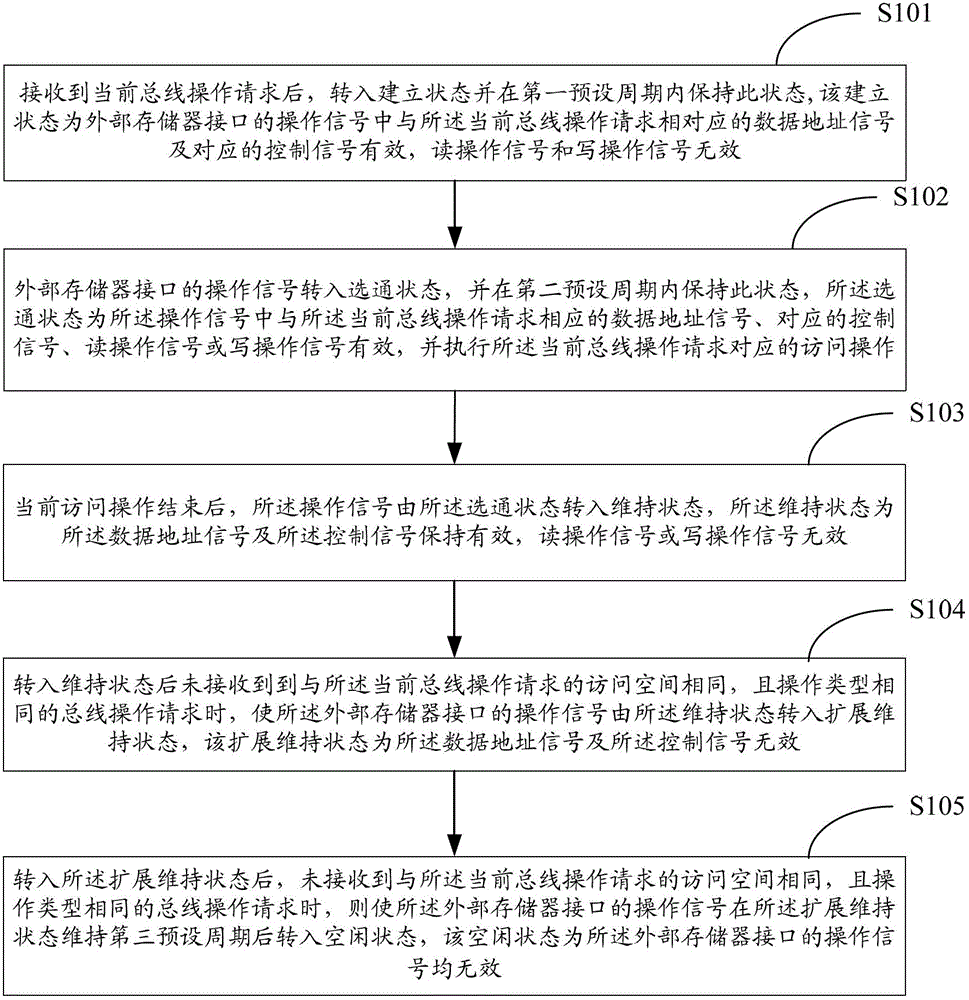
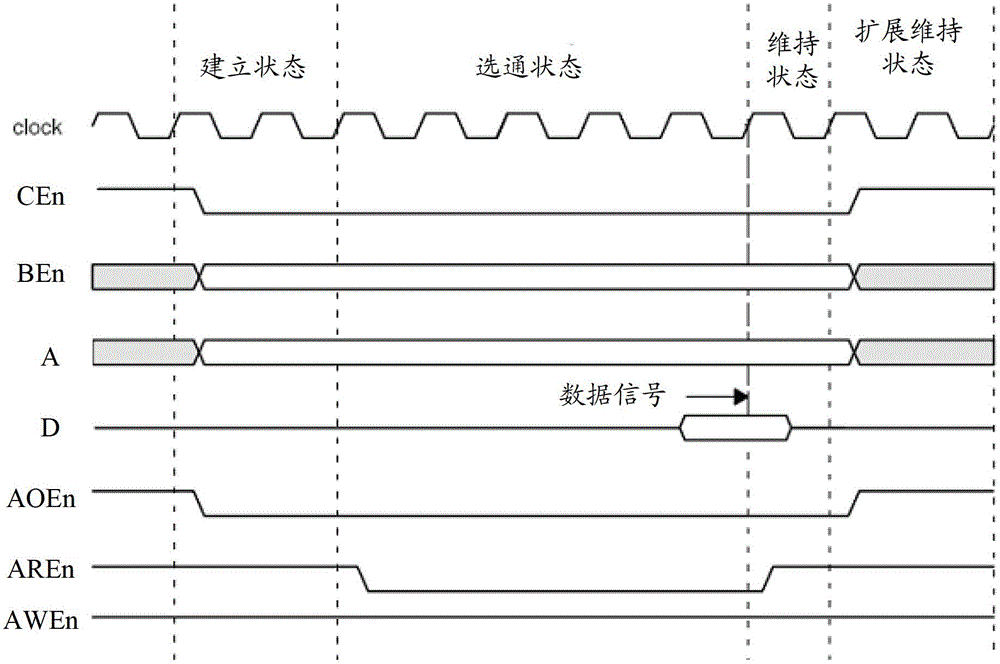
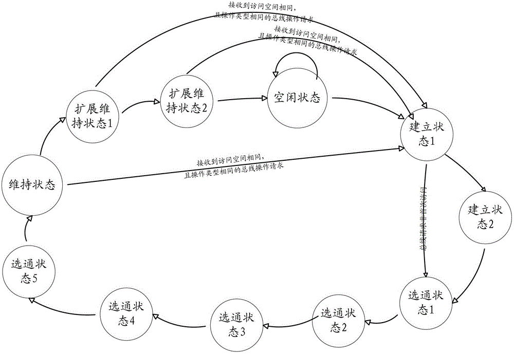
[0018] The bus interface conversion method provided in the embodiment of the present application is used for communication between a wireless communication module based on an external memory interface and a system-on-chip based on an AMBA bus. The AMBA bus includes a system bus AHB (Advance High-performance Bus, advanced high-performance bus ) and peripheral bus APB (Advance Peripheral Bus, advanced peripheral bus). The bus interface conversion method is used to convert the bus operation request of the system-on-chip to operate the wireless communication module into a timing state based on an external memory interface that the wireless communication module can recognize. Specifically, the method includes: According to the received bus operation request, generate an operation signal conforming to the timing state of the external memory interface, and perform corresponding operations, wherein the timing state of the external memory interface includes: idle state, setup state, str...


PUM


Abstract

The invention discloses a bus interface conversion method and a bus bridging device. The bus interface conversion method is specifically characterized by comprising the steps of generating operation signals according with the timing sequence states of an interface of an external memory according to the received bus operating requirements, and executing the corresponding operation so as to establish the communication between a system on a chip on the basis of the bus and a wireless communication module based on the interface of the external memory, wherein the timing sequence states of the interface of the external memory comprise an idle state, an establishment state, a gating state, a maintenance state, and an extended maintenance state. In this way, when a wireless communication module processed verified by FPGA (field programmable gate array) is transplanted to the system on the chip on the basis of an AMBA (advanced microcontroller bus architecture) bus, bus read-write operation requirements can be converted into the read-write operation time sequence of the interface of the external memory, the redesign to the AMBA bus interface of the wireless communication module can be avoided, the verification period is shortened after the wireless communication module is integrated to the system on the chip on the basis of the AMBA bus, and the cost of the system on the chip on the basis of the AMBA bus is lowered.

Description

technical field [0001] The present application relates to the field of system-on-chip technology, in particular to a bus interface conversion method and a bus bridge device. Background technique [0002] With the development of semiconductor technology, system-on-chip has become the mainstream technology today. The system-on-chip generally integrates one or more functional modules based on the system-on-chip bus. At present, the mainstream system-on-chip bus standards include Core Connect bus, AMBA (Advanced Microcontroller Bus Architecture, advanced microprocessor bus architecture) bus, OCP (Open Core Protocol Specification, open core protocol) and Wishbone bus, among them, AMBA on-chip bus is widely used in high-performance embedded because of its rich IP core resources and simple operation protocol system. [0003] Usually, in a wireless communication system on a chip, in addition to integrating a CPU and a wireless communication function module, a DSP (Digital Signal Pr...

Claims


Application Information

Patent Timeline
Patent Type & Authority Applications(China)
IPC IPC(8): G06F13/16
Inventor 冯燕陈岚
Owner INST OF MICROELECTRONICS CHINESE ACAD OF SCI
Why Eureka
Try Eureka