Design method of contact type card verification system based on FPGA (field programmable gate array)

A verification system and card design technology, applied in computing, instruments, electrical digital data processing, etc., can solve the problems of high cost of chip tape-out, insufficient verification reliability, etc.

Inactive Publication Date: 2012-06-13
SHANDONG UNIV
View PDF3 Cites 2 Cited by
  • Summary
  • Abstract
  • Description
  • Claims
  • Application Information

AI Technical Summary

Problems solved by technology

[0012] Aiming at the problems of increasing verification complexity of integrated circuit chips, insufficient verification reliability, high cost of chip tape-out, and how to shorten the design cycle, the present invention provides a design method of an FPGA-based contact card verification system

Method used


Image

  • Design method of contact type card verification system based on FPGA (field programmable gate array)
  • Design method of contact type card verification system based on FPGA (field programmable gate array)
  • Design method of contact type card verification system based on FPGA (field programmable gate array)

Examples


Embodiment

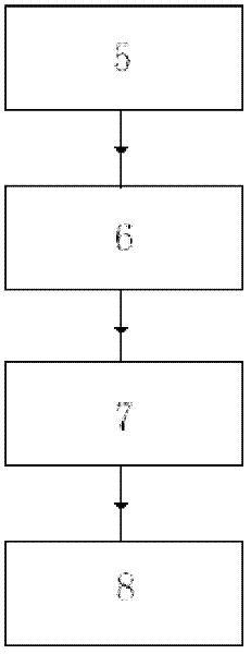
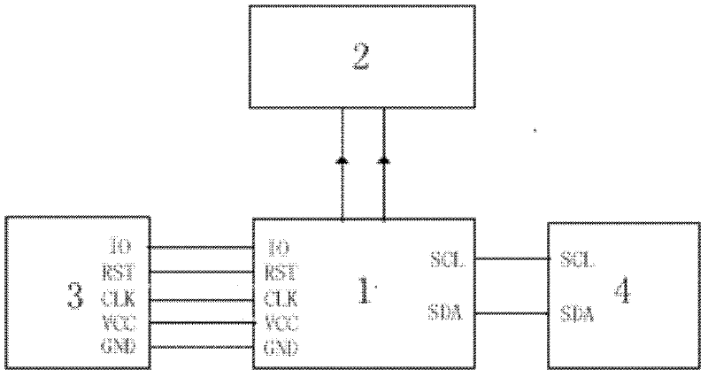
[0034] A design method of a FPGA-based contact card verification system, such as figure 1 , figure 2 As shown, the steps are as follows:

[0035] 1) Select FPGA as the design platform for the verification system;

[0036] 2) Transplant the contact card design on the FPGA platform, mainly including IO processing and IP replacement:

[0037] IO processing: According to the contact card design specification, modify the IO port of the contact card design in the FPGA platform, so that the IO port conforms to the interface specification in the ISO-7816 protocol;

[0038] IP replacement: replace the IP core based on the integrated circuit design process in the contact card design with the IP core suitable for the FPGA platform according to the functions realized by the IP core;

[0039] 3) Build the verification system environment:

[0040] The verification system environment includes a card reader conforming to the ISO-7816 protocol, EEPROM data storage chip, FPGA platform for ...


PUM


Abstract

A design method of a contact type card verification system based on an FPGA (field programmable gate array) belongs to the technical field of verification of integrated circuit chips, aims to solve problems of high complexity of verification operation, slow simulation speed of software, insufficient reliability and the like of verification of integrated circuits in the prior art, and is applied to integrated circuit design. The verification system based on the FPGA adopts the design of a contact type card as a verification object, and has the advantages of high reliability, fast simulation speed, high portability and reconfigurability and the like, problems of high test complexity, slow simulation speed, insufficient reliability, complication in modification and the like in traditional verification of the integrated circuits are solved, and a new solution can be provided for verification technology of the integrated circuit design.

Description

technical field [0001] The invention relates to a design method of an FPGA-based contact card verification system, belonging to the technical field of integrated circuit chip verification. Background technique [0002] With the continuous upgrading of electronic products and the progress of semiconductor technology, the design scale of integrated circuit chips continues to increase, which poses new challenges to the design of integrated circuit chips: [0003] 1) Shorten the design cycle of the chip and speed up the time to market of the product, thereby improving the competitiveness of the product. [0004] 2) Improve the success rate of one-time casting of the chip, thereby reducing the cost of tape-out. [0005] In the integrated circuit chip design cycle, the verification work of the chip occupies 60-70% of the design workload, and with the continuous increase of the chip scale, the complexity of chip verification continues to increase, and the difficulty of verificatio...

Claims


Application Information

Patent Timeline
Patent Type & Authority Applications(China)
IPC IPC(8): G06F17/50
Inventor 周莉章元智王佳汪建军康晓
Owner SHANDONG UNIV
Why Eureka
Try Eureka