Masking template, static random access storage unit and storage

A technology of static random access and storage unit, which is applied in the direction of electrical components, electric solid-state devices, semiconductor devices, etc. It can solve problems such as chamfering and affecting device performance, and achieve the effect of simple production and avoiding mismatching problems

Active Publication Date: 2012-10-10
SHANGHAI HUAHONG GRACE SEMICON MFG CORP
View PDF6 Cites 2 Cited by
  • Summary
  • Abstract
  • Description
  • Claims
  • Application Information

AI Technical Summary

Problems solved by technology

However, when the driving NMOS transistor is actually made larger than the access NMOS transistor, a certain degree of chamfering will inevitably

Method used


Image

  • Masking template, static random access storage unit and storage
  • Masking template, static random access storage unit and storage
  • Masking template, static random access storage unit and storage

Examples


Embodiment Construction

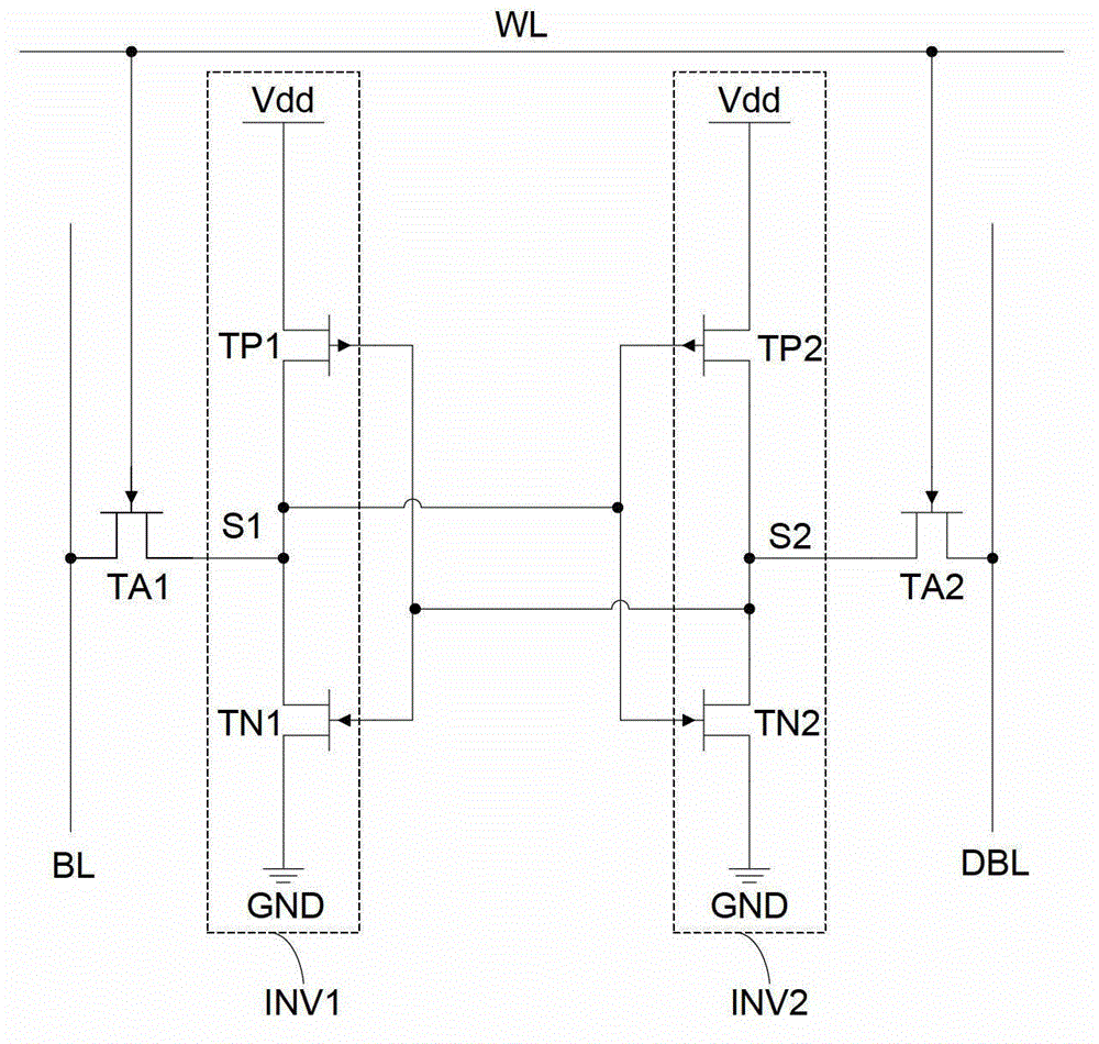
[0036] In order to ensure the normal operation of the storage unit of the SRAM in the existing technology, the size of the access NMOS transistor in the storage unit must be larger than that of the driving NMOS transistor to obtain a β value (beta ratio).

[0037]The larger the size difference between the two, the larger the beta ratio; and the larger the beta ratio value, the higher the stability of the storage unit.

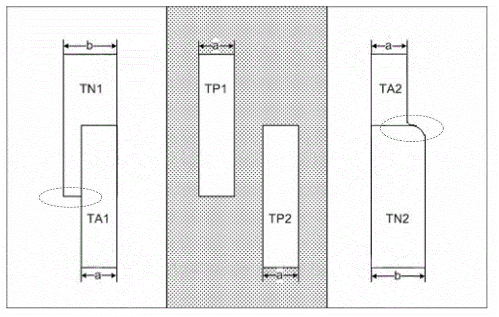
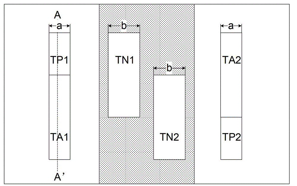
[0038] figure 2 is a schematic top view of a conventional reticle with static random access memory cell patterns. Such as figure 2 As shown, the first load PMOS transistor TP1 pattern, the first access NMOS transistor TA1 pattern, the second load PMOS transistor TP2 pattern, and the second access NMOS transistor TA2 pattern have the same first critical dimension a. The pattern of the first driving NMOS transistor TN1 and the pattern of the second driving NMOS transistor TN2 have the same second critical dimension b. In order to obtain the above betaratio, ...


PUM


Abstract

Provided is a masking template with a static random access storage unit graph, a static random access storage unit and a storage. The masking template comprises at least one access N-channel metal oxide semiconductor (NMOS) transistor graph and at least one loading p-channel metal oxide semiconductor (PMOS) transistor graph, the access NMOS transistor graph and the loading PMOS transistor graph are equal in quantity and provided with same first critical dimension, and the access NMOS transistor graph and the loading PMOS transistor graph are arranged in pair and are connected face to face in the direction of the first critical dimension. The static random access storage unit comprises at least one access NMOS transistor and least one loading PMOS transistor, the access NMOS transistor and the loading PMOS transistor are equal in quantity and provided with same first critical dimension, the access NMOS transistor and the loading PMOS transistor are located on a substrate and arranged in pair, and the access NMOS transistor and the loading PMOS transistor are connected face to face in the direction of the first critical dimension. The storage comprises the storage unit. The masking template, the static random access storage unit and the storage are simple and convenient and have no influences on device performance.

Description

technical field [0001] The invention relates to the technical field of semiconductor manufacturing, in particular to a reticle with a pattern of a static random access memory unit, a static random access memory unit and a memory. Background technique [0002] According to the different ways of storing data, semiconductor memory can be divided into two categories: random access memory (RAM) and read-only memory (ROM). Random access memory (RAM) can be divided into static random access memory (SRAM) and dynamic random access memory (DRAM). Compared with DRAM, SRAM has faster read and write speeds. Moreover, SRAM does not need to periodically refresh the stored information, and its design and manufacture are relatively simple. [0003] The overall structure of SRAM can be divided into two parts: memory bank array and peripheral circuit. Wherein, the memory bank array is composed of a precharge circuit and a memory cell array. In SRAM, the storage unit is its most basic and ...

Claims


Application Information

Patent Timeline
IPC IPC(8): H01L27/02H01L27/11
Inventor 胡剑
Owner SHANGHAI HUAHONG GRACE SEMICON MFG CORP
Why Eureka
Try Eureka