Mirror image rejection down-conversion receiving system and method based on photoelectric oscillator

A photoelectric oscillator and image suppression technology, which is applied in the field of optical communication, can solve the problems of IM suppression performance degradation and achieve the effects of avoiding mismatch problems, low power consumption, and high-performance optical down-conversion output

Active Publication Date: 2022-02-25
AIR FORCE EARLY WARNING ACADEMY
10 Cites 0 Cited by

AI-Extracted Technical Summary

Problems solved by technology

Although this type of method has the advantage that the applicable frequency is not limited, it also has the problem of reduced IM suppressi...

Abstract

The invention discloses a mirror image rejection down-conversion receiving system and method based on a photoelectric oscillator, and mainly relates to the field of optical communication and the technical field of microwave photons. The system comprises a photoelectric oscillator loop and a down-conversion oscillation loop, the photoelectric oscillator loop comprises a laser, a first phase modulator, an optical amplifier, a first optical circulator, a first phase shift Bragg grating, a first photoelectric detector and an electric coupler, and selective amplification receiving of radio frequency input signals is achieved; and the down-conversion oscillation loop comprises a second phase modulator, a second circulator, a second phase shift Bragg grating, a second photoelectric detector, an electric amplifier and an electric beam splitter, and down-conversion output of the radio frequency input signal is realized. The beneficial effects of the invention are that the system does not need external local oscillator signal source input, the input IM signal is filtered through the frequency selection characteristic of the photoelectric oscillator, the 'mismatch problem' in the phase cancellation technology can be avoided, and the applicable frequency range can be tuned by tuning the frequency of the laser.

Application Domain

Technology Topic

Radio frequencyOpto-electronic oscillator +22

Image

  • Mirror image rejection down-conversion receiving system and method based on photoelectric oscillator
  • Mirror image rejection down-conversion receiving system and method based on photoelectric oscillator
  • Mirror image rejection down-conversion receiving system and method based on photoelectric oscillator

Examples

  • Experimental program(1)

Example Embodiment

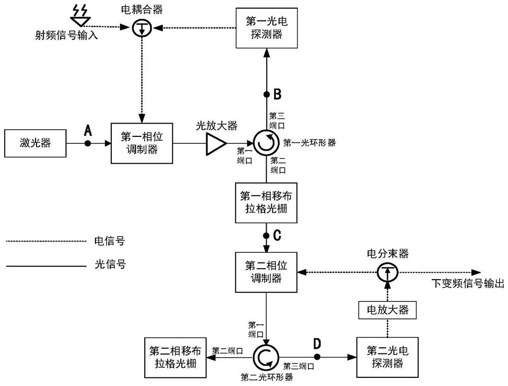
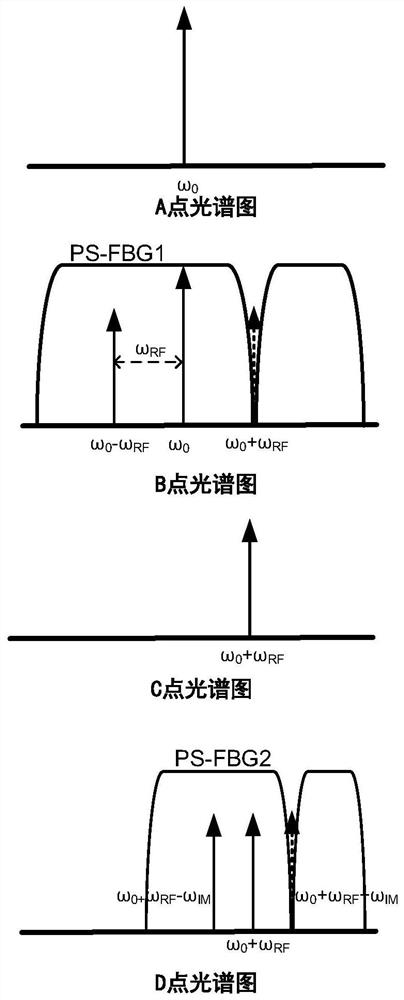
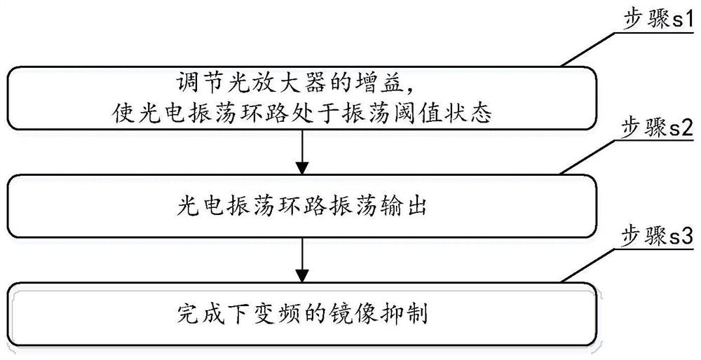
[0020] In order to make the objects and advantages of the present invention, the present invention will be further described below in connection with the embodiments;
[0021] A preferred embodiment of the present invention will be described below with reference to the accompanying drawings. It will be understood by those skilled in the art that these embodiments are merely illustrative of the technical principles of the invention, and are not intended to limit the scope of the invention.
[0022] It should be noted that the term "upper", "lower", "left", "left", ",", ",", ",", ",", ",",, is, based on the figures The direction or positional relationship is shown, which is merely intended to be described, rather than indicating or implying that the device or element must have a specific orientation, and is not understood to limit the limitation of the invention.
[0023]Further, it is also necessary to explain that in the description of the present invention, the term "mount", "connected", "connection",, unless otherwise express, "Connect", "Connect",,,,,,,,,,,,,,,,,,,,,,,,,,,,,,,,,,,,,,,,,,,,,,,,,,,,,,, It is a detachable connection, or integrally connected; it can be a mechanical connection, or an electrical connection; it can be directly connected, or can be interconnected by an intermediate medium, which may be in the interior of the two elements. The specific meaning of the above terms in the present invention can be understood from the particular circumstances.
[0024] The present invention provides a mirror-based inhibition of photoelectric oscillators, and the system includes a photoelectric oscillator loop and a down-frequency oscillation loop. Photoelectric oscillator loop includes a laser, a first phase modulator, a light amplifier, a first photoembol, a first phase shift grating, a first photodetector, and an electrical adjuster; wherein the output of the laser is from the first phase. The light input of the modulator is connected, and the light output terminal of the first phase modulator is connected to the light input terminal of the optical amplifier, and the output of the optical amplifier is connected to the first port of the first annular ring, and the first annular end The two port is connected to the light input terminal of the first phase shift brigade grating, and the third port of the first photolode is connected to the light input of the first photodetector, and the output terminal and electrical adjuster of the first photodetector. One of the ports are connected, and the output of the electrical adjuster is connected to the radio frequency input of the first phase modulator, and the other port of the electrical coupler is used to input a radio frequency signal. The lower variable frequency oscillation loop includes a second phase modulator, a second photoelectric annulus, a second phase shift, a second photodetector, an electrical amplifier, an electro-bundrel; wherein the light output of the first phase shift. The light input terminal of the second phase modulator is connected, and the light output terminal of the second phase modulator is connected to the first port of the second photoelectric annular, and the second port of the second photoelectric ring and the second phase shift. The input end is connected, the third port of the second photoelectric ring is connected to the light input terminal of the second photodetector, and the output of the second photodetector is connected to the input of the electric amplifier, and the output terminal and an electrical component of the electrical amplifier are connected. The input of the beam is connected, and an output of the electro-bundrel is connected to the input of the second phase modulator, and an additional output of the electro-bundrel outputs a downconvert signal.
[0025] The schematic diagram of the mirroring inhibition of photoelectric oscillators, for reference figure 1 Indicated. The operating principle of the system is: the laser generates the optical carrier to modulate the RF signal to the optical carrier, thereby forming a light phase modulation signal. The first photoelectric annular and the first phase shift grating constitute a notch filter to achieve a +1 step edge filter of the optical phase modulation signal, i.e., the light reflection spectrum of the first phase shift bridal grating via the first annulus. The third port output. The third port output of the first photoembolizer is output by the first photodetector after the first photodetector is demodulated. The radio frequency signal output by the first photoelectric detector is input to the first phase modulator to form an optical signal transmission loop through the electrical coupling device, so that photoelectric oscillation can be realized. The gain of controlling the light amplifier makes the output oscillator mode in a critical state. When the input radio frequency signal frequency is the same as the photographic oscillator output signal frequency, the weak radio frequency signal input can cause the photoelectric oscillator to activate the output, so that the first phase The port is transferred to the +1 step strip of the light phase modulation signal. The first Prague grating transmitted + 1-step strip is lost to the second phase modulator as the optical carrier. The second photoelectric annular and the second phase shift port constitutes a notch filter that implements the phase-intensity conversion of the optical phase modulation signal by filtering. The third port of the second photoelectric annular outputs the light reflection spectrum of the second phase shift bridal grating, and is finally transmitted to the second photodetector to achieve demodulation. Electrical amplifier amplifies demodulation signal. The electro-bundrel divides the amplified demodulation signal into two channels, all the way to the second phase modulator constituting an oscillation loop, and the lower frequency conversion signal output is achieved.
[0026] The present invention provides a method of frequency conversion receiving method based on an optoelectronic oscillator, please refer to image 3 As shown, you can implement it as follows:
[0027] Step 1: The output frequency of the laser is expressed as Ω 0 , The optical signal output by the laser is as figure 2 The A-point spectrum is shown; the transmission notch position frequency of the first phase shift grating is expressed as Ω 1 However, the photoelectric oscillator loop composed of a laser, a first phase modulator, a light amplifier, a first photoelectric detector, a first phase shift, a first photodetector, and an electrical coupler can generate a frequency Ω. 1 ω 0 The radio frequency signal, the gain of adjusting the optical amplifier makes the photoelectric oscillation loop in the oscillation threshold state;
[0028] Step 2: When the frequency ω of the radio frequency signal is input RF = Ω 1 ω 0 When the photoelectric oscillation loop oscillation output, the optical signal output of the reflected port output of the first phase shift bridal grating is like figure 2 The B-Point Spectrum Schematic is shown, including the frequency Ω 0 The optical carrier and frequency-1-1-step radial light beam; the transmitted port output of the first phase shift port is output. figure 2 The C-point spectrum is shown in the picture, only the frequency is Ω. 0 + Ω RF +1 step raw frequency beam; when the frequency of the radio frequency signal is input RF ≠ Ω 1 ω 0 When the photoelectric oscillation loops cannot be oscillated.
[0029] Step 3: The +1 step-race radial sideband is input as the optical carrier to the second phase modulator to achieve phase modulation; the transmission notch position frequency of the first phase shift grating is expressed as Ω 2 However, the lower variable frequency oscillation loop composed of the second phase modulator, the second annulus, the second phase shift, the lower variable frequency oscillation loop, and the oscillation of the lower variable-frequency oscillation loop configuration. Output, the optical signal of the final input of the second photodetector is as figure 2 The D-point spectrum is shown in the schematic diagram of the shooting, the port output frequency of the electric bundle is Ω. RF ω 2 (Ω RF ≠ Ω 2 The lower frequency conversion signal; for the output frequency Ω RF ω 2 The lower frequency output signal, the input signal frequency of the mirror interference is 2Ω 2 ω RF , But 2Ω 2 ω RF ≠ Ω RF , Input frequency is 2Ω 2 ω RF The mirror interference signal cannot achieve the lower frequency conversion output, thus realizing mirror suppression in the down-conversion.
[0030] In this embodiment, when the signal input of the mirror frequency is input, the system does not cause the photoelectric oscillator to be output, and the first phase shift brid grating cannot transmit the +1 step mirror frequency sideband, so the mirror frequency signal input will eventually produce. The down-frequency output is achieved, thereby realizing mirror suppression.
[0031] Specifically, by the output frequency of the tuning the laser, selective lower frequency conversion processing on a single radio frequency input frequency can be realized; by selecting the first phase shift port, the transmitting notch frequency position of the second phase shift cabgle, can be selected. The frequency of the final down frequency output signal is fixed.
[0032] Here, the technical solution of the present invention has been described in connection with the preferred embodiment shown in the drawings, but those skilled in the art is that the scope of the invention is clearly not limited to these specific embodiments. Under the preparation of the present invention, those skilled in the <
[0033] It is not intended to limit the invention as described above, and is not intended to limit the invention; for those skilled in the art, the present invention can have various changes and variations. Any modification, equivalent replacement, improvement, etc. according to the present invention should be included within the scope of the invention.

PUM

no PUM

Description & Claims & Application Information

We can also present the details of the Description, Claims and Application information to help users get a comprehensive understanding of the technical details of the patent, such as background art, summary of invention, brief description of drawings, description of embodiments, and other original content. On the other hand, users can also determine the specific scope of protection of the technology through the list of claims; as well as understand the changes in the life cycle of the technology with the presentation of the patent timeline. Login to view more.

Similar technology patents

Method of fabricating circuit on ductile flexible substrate

ActiveCN107278040AAvoid mismatch problemsOvercoming crack and open circuit problemsLithography/patterningConductive material chemical/electrolytical removalCopper foilResist
Owner:SHANDONG UNIV OF SCI & TECH

Classification and recommendation of technical efficacy words

  • Avoid mismatch problems

Method of fabricating circuit on ductile flexible substrate

ActiveCN107278040AAvoid mismatch problemsOvercoming crack and open circuit problemsLithography/patterningConductive material chemical/electrolytical removalCopper foilResist
Owner:SHANDONG UNIV OF SCI & TECH
Why Eureka
Try Eureka