BE-SONOS (bandgap engineered-SONOS) structural device with low compile voltage and trapping charge and forming method of BE-SONOS structural device

A BE-SONOS and voltage technology, applied in the field of microelectronics, can solve problems affecting device performance, erasure cannot be performed, etc., and achieve the effect of reducing capture and suppressing unstable factors

Active Publication Date: 2014-11-19
SHANGHAI HUALI MICROELECTRONICS CORP
View PDF4 Cites 0 Cited by
  • Summary
  • Abstract
  • Description
  • Claims
  • Application Information

AI Technical Summary

Problems solved by technology

The injected electrons and the holes injected from the substrate achieve a dynamic balance, causing the saturation of the erased state. If the voltage is higher, the erasing cannot be performed, which will affect the performance of the device.

Method used


Image

  • BE-SONOS (bandgap engineered-SONOS) structural device with low compile voltage and trapping charge and forming method of BE-SONOS structural device
  • BE-SONOS (bandgap engineered-SONOS) structural device with low compile voltage and trapping charge and forming method of BE-SONOS structural device
  • BE-SONOS (bandgap engineered-SONOS) structural device with low compile voltage and trapping charge and forming method of BE-SONOS structural device

Examples


Embodiment 1

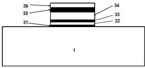
[0023] The process of forming a BE-SONOS structure device with low compilation voltage trapping charges is as follows:

[0024] First prepare a thin silicon oxide layer 31 (referred to as O1) with a thickness of 1.5 nm on the P-type silicon substrate 1, and then prepare a layer of nitrogen-rich nitrogen with a thickness of 2.0 nm on the silicon oxide layer 31. Silicon nitride layer 32 (denoted as rich-N1), the Si / N concentration in the formed silicon nitride layer is 0.1. Then another silicon oxynitride layer 33 (referred to as SiON) with a thickness of 2.5 nm is prepared on the nitrogen-rich silicon nitride layer 32 (rich-N1). Then prepare a layer of 7nm thick silicon nitride layer 34 (denoted as N2) with charge storage capability on the silicon oxynitride layer 33, and thermally oxidize a layer of 9nm thick blocking oxide layer 35 on the layer of charge storage nitride layer (denoted as O3), and finally a polysilicon control gate 36 is prepared on the blocking oxide layer (...

Embodiment 2

[0029] This example is slightly different from Example 1. By adjusting the thickness ratio of nitrogen-rich silicon nitride and N1, the N1 layer with a thickness of 2-t nm in the original BE-SONOS is replaced with a layer of t nm-rich silicon nitride with a thickness of t nm. Nitrogenated silicon nitride layer 32 .

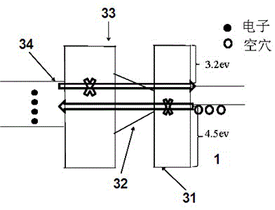
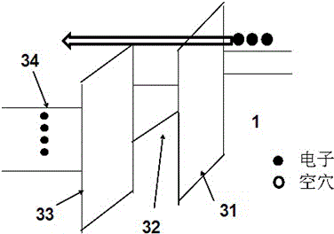
[0030] The obvious erasing speed is due to the fact that the hole barrier (<1.9eV) at the interface between silicon and silicon nitride is smaller than that at the interface between silicon and silicon oxide (4.6eV). At high field, this large barrier difference for holes can produce a large energy band shift under electric field, so that holes only tunnel quickly through the O1 layer.


PUM


Abstract

The invention provides a B E-SONOS (bandgap engineered-SONOS) structural device with low compile voltage and trapping charge. A gate which is in a multiple-layered structure is disposed on the silicon substrate. The gate comprises from bottom to top, a silicon oxide layer (31), a silicon nitride layer (32) containing rich nitrogen, a silicon oxide layer (33), a silicon nitride layer (34), an oxidation resisting layer (35) and a control gate. The silicon oxide layer is contacted with the silicon substrate.

Description

Technical field [0001] The invention involves the field of microelectronics technology, and especially involves a Be-Sonos structural device and formation method with a low compile voltage. Background technique [0002] Flash memory is a type of non -easy -to -lose storage device. Traditional flash memory uses polysilicon floating grids to store data. Because polycrystalline silicon is a conductor, the charge stored in the floating grid pole is continuously distributed.When there is a leakage channel, the charge stored on the entire floating gate will be lost through this leakage channel.Therefore, the maximum obstacle to restricting flash memory according to the proportion is that the thickness of its tunnel penetration oxidation layer cannot continue to decrease.Because in the case of thin tunnel penetration, leakage currents caused by direct tunnels and stress will make huge challenges to the leakage control of the memory.The recently developed SONOS structure replaced the ori...

Claims


Application Information

Patent Timeline
Patent Type & Authority Patents(China)
IPC IPC(8): H01L29/792H01L21/336H01L21/28
Inventor 田志
Owner SHANGHAI HUALI MICROELECTRONICS CORP
Why Eureka
Try Eureka