Vertical-external-cavity surface-emitting semiconductor laser with integrated micro lens

A microlens and laser technology, applied in semiconductor lasers, lasers, laser parts, etc., can solve the problems of unstable working state of external cavity structure external cavity mirror, unsatisfactory laser spectral linewidth, and poor mode stability, etc. Large-scale low-cost production, reduced divergence angle, and less impact on the external environment

Inactive Publication Date: 2012-10-10
CHANGCHUN INST OF OPTICS FINE MECHANICS & PHYSICS CHINESE ACAD OF SCI
View PDF2 Cites 13 Cited by
  • Summary
  • Abstract
  • Description
  • Claims
  • Application Information

AI Technical Summary

Problems solved by technology

[0006] The purpose of the present invention is to solve the problems of the existing VCSEL structure with large divergence angle, poor mode stability and unsatisfactory laser spectrum line width, and the traditional VECSEL structure used to solve these problems is difficult to manufacture, and the external cavity structure is affected by the environment. The problem that the working state of the external cavity mirror is unstable due to the large size

Method used


Image

  • Vertical-external-cavity surface-emitting semiconductor laser with integrated micro lens
  • Vertical-external-cavity surface-emitting semiconductor laser with integrated micro lens

Examples


Embodiment Construction

[0013] The structure of the present invention will be described in further detail below in conjunction with the embodiments given in the accompanying drawings.

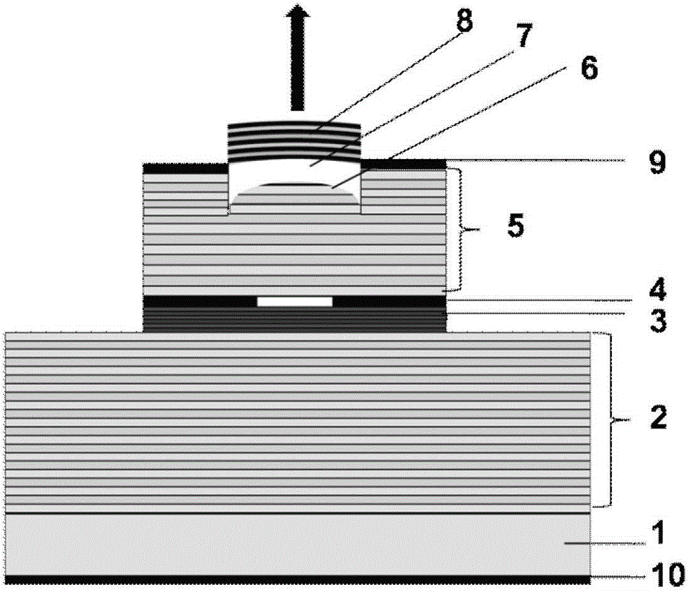
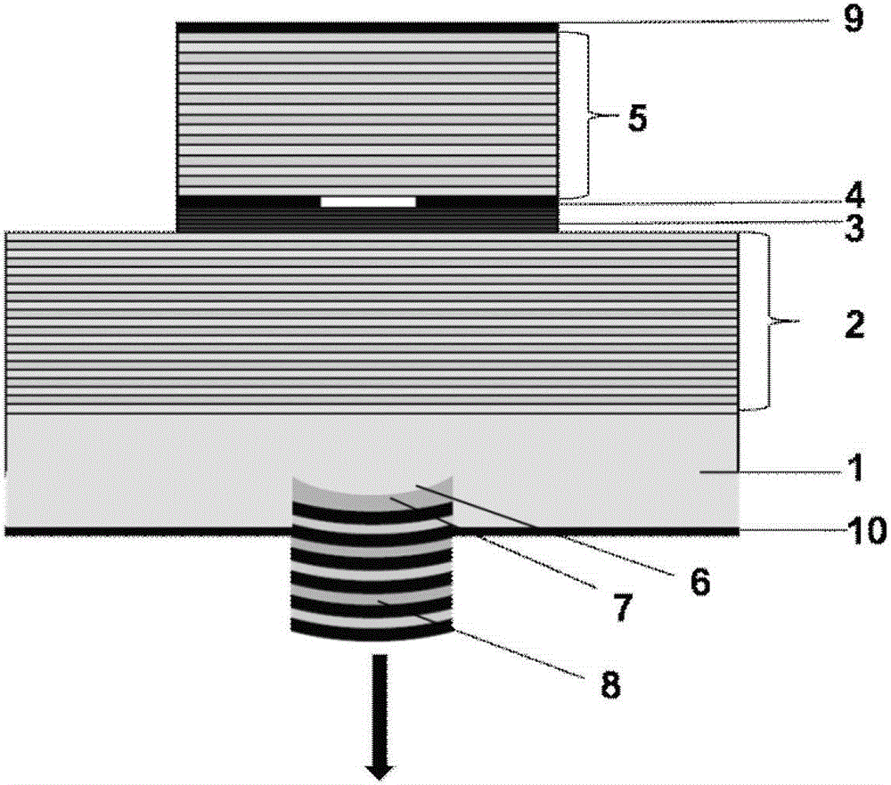
[0014] Such as figure 1 It is shown that the light output from the P surface of the present invention has a microlens integrated VECSEL structure, and the device structure emits laser light from the side of the P-type DBR. The structure from bottom to top is N-face electrode 10, N-type substrate 1, N-type DBR 2, active layer 3, oxidation limiting layer 4, P-type DBR 5, microlens structure 6, external coupling cavity 7, and external cavity DBR Mirror 8, and P surface electrode 9. Both the N-face electrode and the P-face electrode are electrically connected to the device. The microlens structure 6 is a lens shape with a certain curvature directly etched on the P-type DBR. The external coupling cavity 7 and the external cavity DBR mirror 8 are formed after epitaxial growth on the microlens structure 6 .

[0015] Such...


PUM


Abstract

The invention relates to a vertical-external-cavity surface-emitting semiconductor laser with an integrated micro lens and belongs to the technical field of semiconductor optoelectronics. The vertical-external-cavity surface-emitting semiconductor laser solves the problems of high difficulty in structural manufacturing and instability in operation of an existing VECSEL (vertical vertical-external-cavity surface-emitting-laser). The laser comprises an N-face electrode, an N-type substrate, an N-type DBR (distributed bragg reflector), an active layer, an oxidation limiting layer, a P-type DBR, a P-face electrode, a micro lens structure, an external coupled cavity and an external cavity DBR. When the P face is used for light outgoing, the micro lens structure is positioned at a light outlet and formed on the P-type DBR, the external coupled cavity grows on the micro lens structure, and the external cavity DBR grows on the external coupled cavity. When the N face is used for light outgoing, the micro lens structure is positioned at the light outlet and formed on the N-type DBR, the external coupled cavity grows on the micro lens structure, and the external cavity DBR grows on the external coupled cavity. The problem of failure in alignment of an external cavity reflector center to a light outlet center is solved by the integral structure of the vertical-external-cavity surface-emitting semiconductor laser.

Description

technical field [0001] The invention belongs to the technical field of semiconductor optoelectronics, and in particular relates to a vertical external cavity surface-emitting semiconductor laser with integrated microlenses. Background technique [0002] VCSEL is a semiconductor laser that emits light vertically on the surface. It has the advantages of low threshold, high power density, and easy monolithic integration. It has important applications in information storage, space communication, and satellite navigation. With the expansion of application fields, reducing the divergence angle and spectral linewidth of devices has become a research hotspot in recent years. [0003] The existing vertical cavity surface emitting semiconductor laser structure includes N-face electrode, substrate, buffer layer, N-type DBR, active region, oxidation confinement layer, P-type DBR and P-face electrode from bottom to top; due to the uniformity of the DBR structure The reflection character...

Claims


Application Information

Patent Timeline
Patent Type & Authority Applications(China)
IPC IPC(8): H01S5/183
Inventor 张建伟宁永强刘云秦莉王立军
Owner CHANGCHUN INST OF OPTICS FINE MECHANICS & PHYSICS CHINESE ACAD OF SCI
Why Eureka
Try Eureka