Electronic product and liquid crystal varifocus lens thereof

A liquid crystal zoom lens and liquid crystal layer technology, applied in nonlinear optics, instruments, optics, etc., can solve the problems of reducing production cost, complex process, increasing structural design difficulty, etc., and achieve the effect of reducing production cost and reducing process difficulty

Active Publication Date: 2012-10-17
TRULY SEMICON
View PDF5 Cites 32 Cited by
  • Summary
  • Abstract
  • Description
  • Claims
  • Application Information

AI Technical Summary

Problems solved by technology

[0004] However, the liquid crystal zoom lens also has certain defects: according to the liquid crystal refractive index control principle of the liquid crystal cell, the equivalent resistance of the annular wave zone and the conductive medium 32 should be kept equal; figure 1 As shown, the width of each ring-shaped zone electrode is equal, and the conductive medium 32 between adjacent ring-shaped zone electrodes is fan-shaped, so the difficulty of structural design is increased when the above requirements are realized, and the process is also relatively complicated, which is not conducive to reducing Cost of production

Method used


Image

  • Electronic product and liquid crystal varifocus lens thereof
  • Electronic product and liquid crystal varifocus lens thereof
  • Electronic product and liquid crystal varifocus lens thereof

Examples


Embodiment 1

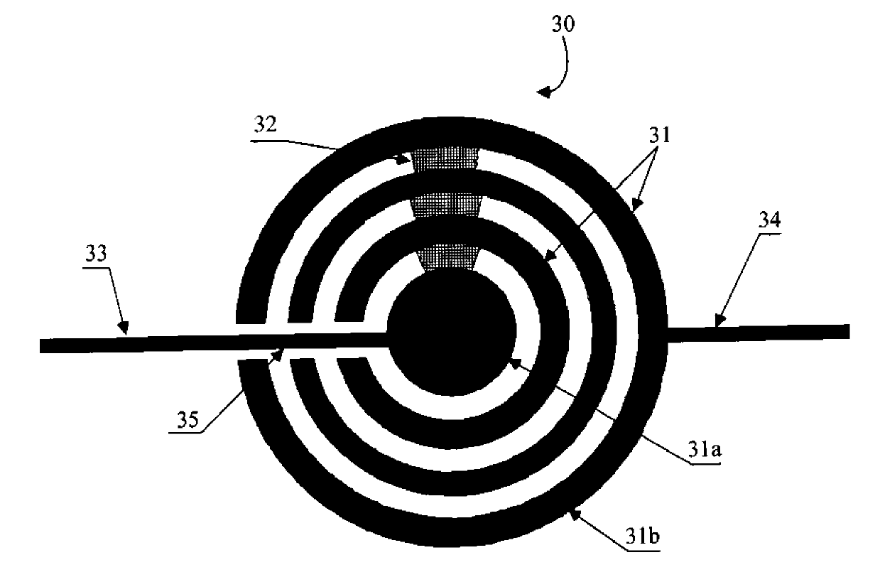
[0054] see Figure 3a ~ Figure 3e , represents the first embodiment of the electrode pattern. A plurality of ring-shaped wave-zone electrodes 141 are arranged on the first surface electrode 140, wherein the width value of each ring-shaped wave-zone electrode 141 decreases gradually from the inside to the outside, specifically according to the width value of the nth ring-shaped wave-zone electrode according to distribution; adjacent ring-shaped band electrodes 141 are insulated and separated, specifically the first surface electrode 140 etches an insulating gap 142 between adjacent bands, and the insulating gap is as small as possible, preferably with a width of Below 10 μm (more preferably below 5 μm); Connect with equivalent resistance between adjacent ring-shaped wave zone electrodes 141, and lead out through the first lead electrode 160 and the second lead electrode 170, wherein the first lead electrode 160 and the second lead electrode 170 The second lead electrodes 170...

Embodiment 2

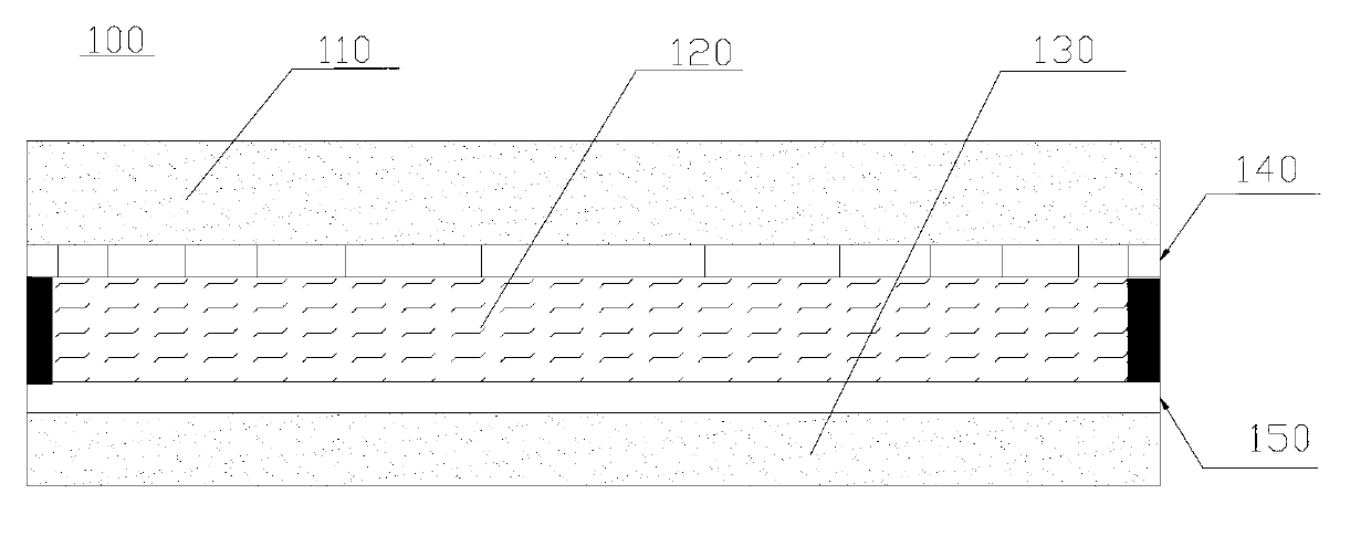
[0060] see Figure 4a ~ Figure 4c , represents the second embodiment of the electrode pattern. The difference from Embodiment 1 is that the concentric ring-shaped zone electrode 141, the first lead electrode 160, and the second lead electrode 170 are respectively formed with two layers of transparent conductive materials, and a transparent insulating layer 180 is used between the two layers of transparent conductive material layers. The insulation is separated, wherein: one layer of transparent conductive material is used to form the Fresnel zone pattern, and the other layer of transparent conductive material is used to form the first lead electrode 160 and the second lead electrode 170 .

[0061] The transparent insulating layer 180 can cover the entire Fresnel pattern area or only cover the area where the first lead electrode 160 and the second lead electrode 170 pass, and the transparent insulating layer only covers the first lead electrode and the second lead electrode and...

Embodiment 3

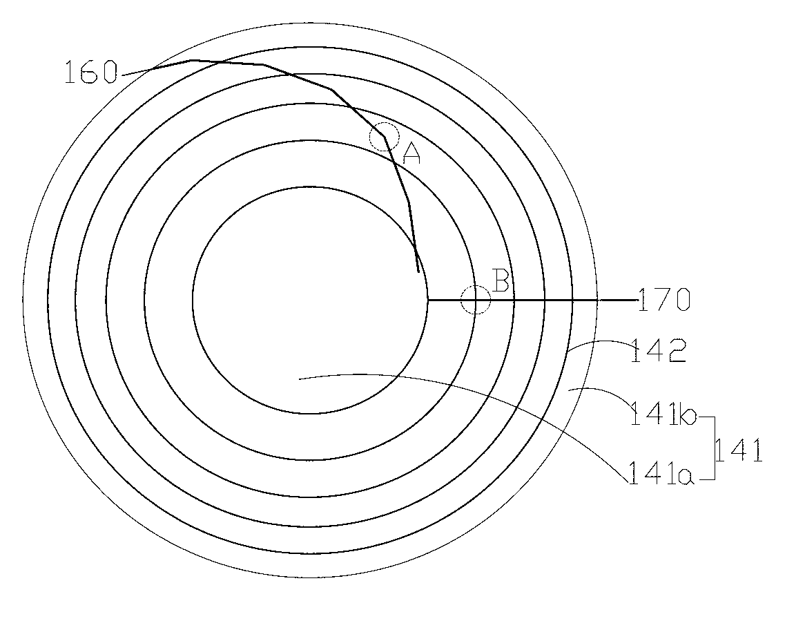
[0065] see Figure 5a ~ Figure 5e , represents the third embodiment of the electrode pattern. Same as the second embodiment, the ring-shaped zone electrode 141 and the first lead electrode 160 and the second lead electrode 170 are respectively formed with two layers of transparent conductive materials, and the two layers of transparent conductive material layers are insulated and separated by a transparent insulating layer 180 The difference is that the transparent insulating layer 180 only covers the first lead electrode 160 and the area outside the conduction junction between the second lead electrode 170 and the ring-shaped zone electrode 141 .

[0066] Wherein: the first lead electrode 160 is designed to have a line width beyond the coverage of the transparent insulating layer at the position where each ring-shaped zone electrode 141 overlaps, and is connected with the corresponding ring-shaped zone electrode 141 to form a conductive junction point, the first lead wire 16...


PUM


Abstract

The invention discloses an electronic product and a liquid crystal varifocus lens of the electronic product. A liquid crystal layer is sealed between an upper planar substrate and a lower planar substrate of the liquid crystal varifocus lens; the upper planar substrate and the lower planar substrate are provided with plane electrodes, respectively; corresponding plane electrodes are used as the inner surfaces; at least one of the plane electrodes of the upper planar substrate and the lower planar substrate is formed as a fresnel wave band pattern electrode; in the fresnel wave band pattern electrode, a width value of an nth annular wave band electrode is distributed according to a formula shown in the description (R1 is the radius of the first ring); adjacent annular wave band electrodes are connected through equivalent resistances and are led out through a first lead electrode and a second lead electrode, wherein the two lead electrodes are not intersected. In terms of design, according to the liquid crystal varifocus lens, on the basis that the requirements on liquid crystal lens infraction rate distribution are realized by using the voltage distribution of an electrode material oneself, the structure and the machining process of the substrate electrode are simplified, and the production cost is reduced; and an optical system of the electronic product adopts the liquid crystal varifocus lens so as to have a large continuous varifocus range and good effect.

Description

technical field [0001] The invention relates to optical devices, in particular to a Fresnel type liquid crystal zoom lens and electronic products using the liquid crystal zoom lens. Background technique [0002] Fresnel-type liquid crystal zoom lenses are widely used in various electronic products such as mobile phones and digital cameras. A common Fresnel lens is composed of upper and lower glass plane substrates and a liquid crystal interlayer. The ITO (Indium Tin Oxides, indium tin metal oxide) conductive film on the inner surface of the two plane substrates is etched into a banded electrode structure, and respectively Connect the corresponding ring-shaped zone electrodes with a common straight-zone electrode. By applying a driving voltage to the control electrode, the refractive index of the liquid crystal layer can be controlled, so that a 180° phase shift occurs between the beam passing through adjacent bands and the main focus, thereby realizing zooming within a pred...

Claims


Application Information

Patent Timeline
Patent Type & Authority Applications(China)
IPC IPC(8): G02F1/29G02F1/1343G02F1/1345
Inventor 王东岳毛航超李赣湘梁永超何基强
Owner TRULY SEMICON
Why Eureka
Try Eureka