Electronic product and liquid crystal varifocus lens thereof
A liquid crystal zoom lens and liquid crystal layer technology, applied in nonlinear optics, instruments, optics, etc., can solve the problems of reducing production cost, complex process, increasing structural design difficulty, etc., and achieve the effect of reducing production cost and reducing process difficulty
- Summary
- Abstract
- Description
- Claims
- Application Information
AI Technical Summary
Problems solved by technology
Method used
Image
Examples
Embodiment 1
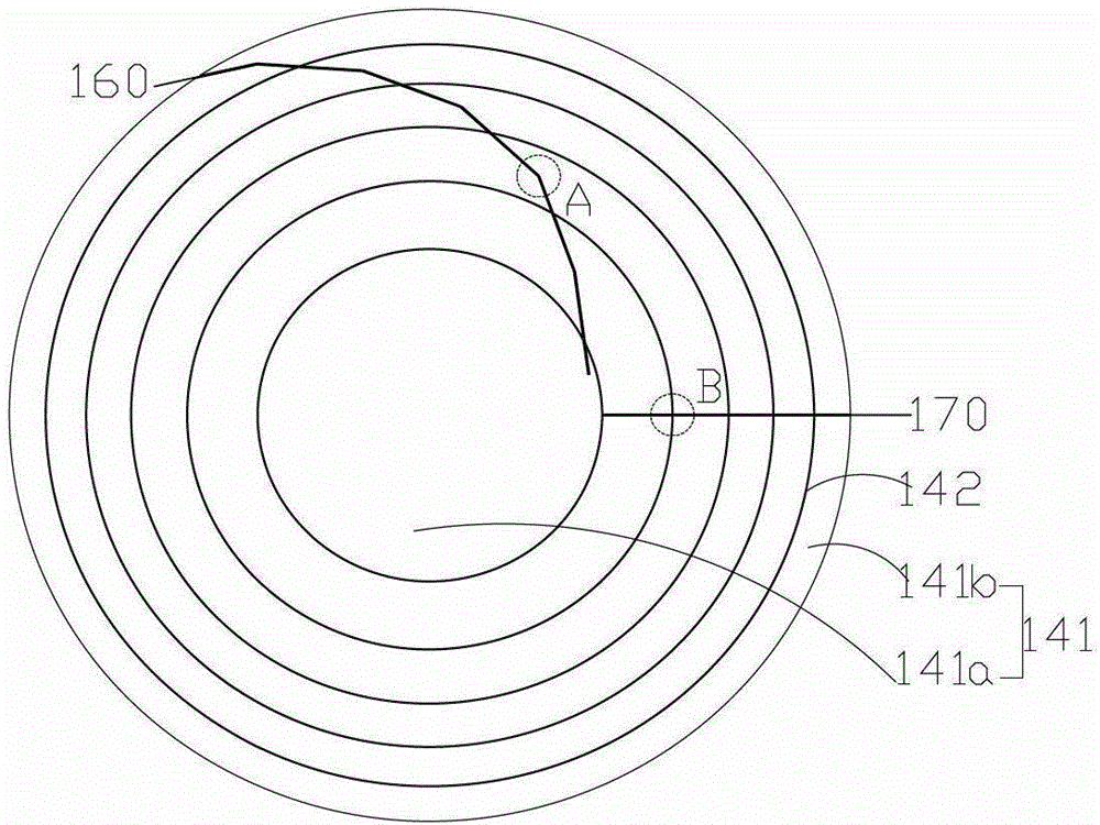
[0054] see Figure 3a ~ Figure 3e , represents the first embodiment of the electrode pattern. A plurality of ring-shaped wave-zone electrodes 141 are arranged on the first surface electrode 140, wherein the width value of each ring-shaped wave-zone electrode 141 decreases gradually from the inside to the outside, specifically according to the width value of the nth ring-shaped wave-zone electrode according to distribution; adjacent ring-shaped band electrodes 141 are insulated and separated, specifically the first surface electrode 140 etches an insulating gap 142 between adjacent bands, and the insulating gap is as small as possible, preferably with a width of Below 10 μm (more preferably below 5 μm); Connect with equivalent resistance between adjacent ring-shaped wave zone electrodes 141, and lead out through the first lead electrode 160 and the second lead electrode 170, wherein the first lead electrode 160 and the second lead electrode 170 The second lead electrodes 170...
Embodiment 2
[0060] see Figure 4a ~ Figure 4c , represents the second embodiment of the electrode pattern. The difference from Embodiment 1 is that the concentric ring-shaped zone electrode 141, the first lead electrode 160, and the second lead electrode 170 are respectively formed with two layers of transparent conductive materials, and a transparent insulating layer 180 is used between the two layers of transparent conductive material layers. The insulation is separated, wherein: one layer of transparent conductive material is used to form the Fresnel zone pattern, and the other layer of transparent conductive material is used to form the first lead electrode 160 and the second lead electrode 170 .
[0061] The transparent insulating layer 180 can cover the entire Fresnel pattern area or only cover the area where the first lead electrode 160 and the second lead electrode 170 pass, and the transparent insulating layer only covers the first lead electrode and the second lead electrode and...
Embodiment 3
[0065] see Figure 5a ~ Figure 5e , represents the third embodiment of the electrode pattern. Same as the second embodiment, the ring-shaped zone electrode 141 and the first lead electrode 160 and the second lead electrode 170 are respectively formed with two layers of transparent conductive materials, and the two layers of transparent conductive material layers are insulated and separated by a transparent insulating layer 180 The difference is that the transparent insulating layer 180 only covers the first lead electrode 160 and the area outside the conduction junction between the second lead electrode 170 and the ring-shaped zone electrode 141 .
[0066] Wherein: the first lead electrode 160 is designed to have a line width beyond the coverage of the transparent insulating layer at the position where each ring-shaped zone electrode 141 overlaps, and is connected with the corresponding ring-shaped zone electrode 141 to form a conductive junction point, the first lead wire 16...
PUM
| Property | Measurement | Unit |
|---|---|---|
| width | aaaaa | aaaaa |
Abstract
Description
Claims
Application Information


