

Semiconductor storage device
A technology of semiconductor and memory unit, applied in the field of dynamic semiconductor storage devices, capable of solving problems such as capacity increase
- Summary
- Abstract
- Description
- Claims
- Application Information
AI Technical Summary
Problems solved by technology
Method used
Image

Examples
no. 1 example
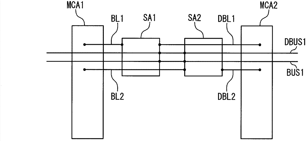
[0057] Figure 5A is a plan view showing the semiconductor layout of the semiconductor integrated circuit device according to the first embodiment of the present invention. Figure 5B is shown by Figure 5A A circuit diagram of the construction of the circuit implemented by the semiconductor layout. First, will describe Figure 5B circuit diagram.
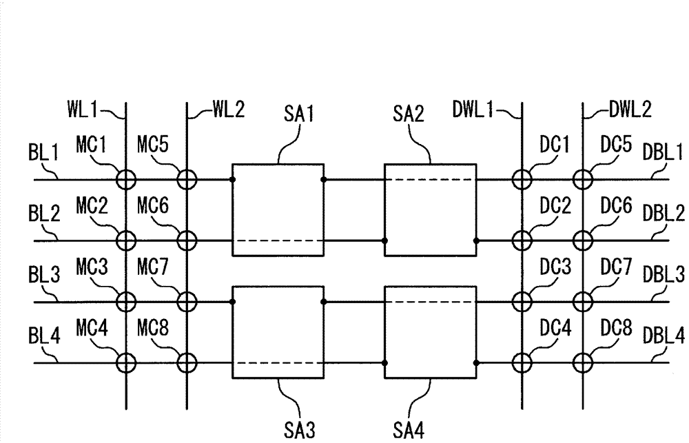
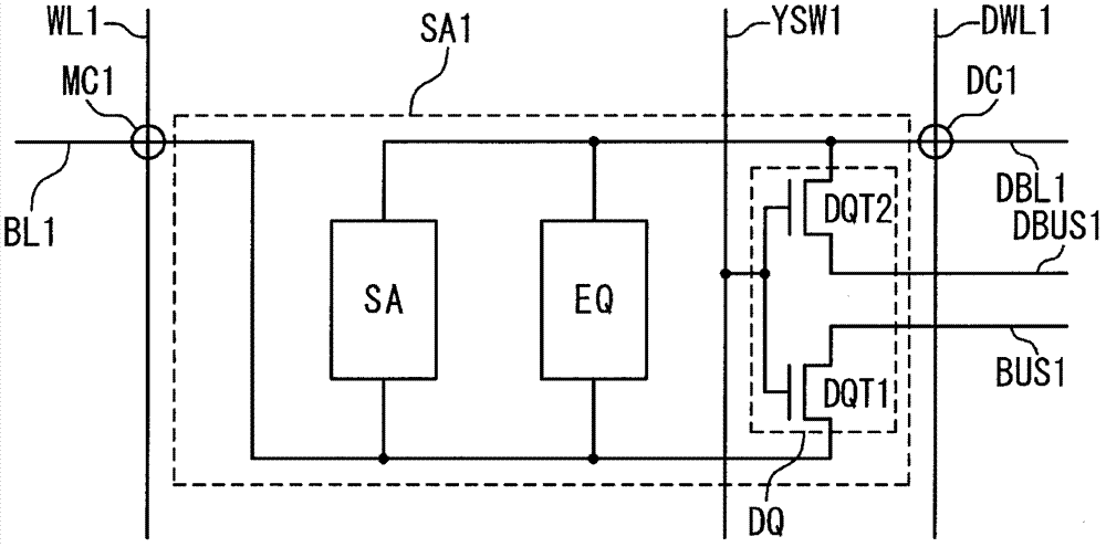
[0058] Figure 5B The circuit diagram is equivalent to that described in the prior art Figure 4A The combination of the two in the circuit diagram. will describe Figure 5B Structural elements in the circuit diagram. Figure 5B The circuit includes first to eighth transfer circuits DQ1 to DQ8, first to eighth column selection signal lines YSW1 to YSW8, bus BUS1, dummy bus DBUS1, first to fourth bit lines BL1 to BL4 and first to fourth Dummy bit lines DBL1 to DBL4.
[0059] The first transfer circuit DQ1 includes a first transistor DQ1T1 and a second transistor DQ1T2. Likewise, the second to eighth transfer circuits DQ2 t...
no. 2 example
[0087] Figure 6 is a plan view showing a semiconductor layout of a semiconductor integrated circuit device according to a second embodiment of the present invention. pass Figure 6 The semiconductor layout implements the circuit with Figure 5B is the same as the first embodiment of the present invention shown in , and thus a detailed description thereof will be omitted. Figure 6 The semiconductor layout of is equivalent to the Figure 5A The semiconductor layout of the first embodiment of the present invention shown in is modified as follows. That is, the positions of the first and second transistors DQ3T1 to DQ6T1 and DQ3T2 to DQ6T2 in the respective third to sixth transfer circuits DQ3 to DQ6 are replaced with each other.
[0088] As an example, the replacement of the positions of the first and second transistors DQ3T1 and DQ3T2 in the third transfer circuit DQ3 will be described in more detail. In the first embodiment, the first transistor DQ3T1 in the third transfe...
no. 3 example
[0102] Figure 7 is a plan view showing a semiconductor layout of a semiconductor integrated circuit device according to a third embodiment of the present invention. pass Figure 7 The semiconductor layout implements the circuit with Figure 5B is the same as the first embodiment of the present invention shown in , and therefore a detailed description will be omitted. Figure 7 The semiconductor layout of is equivalent to the Figure 5A The semiconductor layout of the first embodiment of the present invention shown in is modified as follows. That is, in Figure 5A Among them, two diffusion layers aligned in the longitudinal direction such as the first and third diffusion layers DL1 and DL3 or the second and fourth diffusion layers DL2 and DL4 are shared and changed into one common diffusion layer. Also, refer to Figure 5A , two common diffusion layers aligned in the longitudinal direction such as the first and second common diffusion layers CDL1 and CDL2 are further sha...
PUM
 Abstract
Description
Claims
Application Information