Formation method of Halo structure

A gate structure and ion technology, applied in electrical components, semiconductor/solid-state device manufacturing, circuits, etc., can solve problems such as large fluctuations in device threshold voltage, drift in device characteristics, and inability to meet, and reduce junction capacitance and junction leakage. , the effect of reducing threshold drift and improving electrical characteristics

Inactive Publication Date: 2012-10-17
SEMICON MFG INT (SHANGHAI) CORP
View PDF6 Cites 5 Cited by
  • Summary
  • Abstract
  • Description
  • Claims
  • Application Information

AI Technical Summary

Problems solved by technology

However, as the feature size of the device is further reduced, the Halo structure formed by the phosphorus ion implantation will also produce RSCE (reverse short channel effect) when improving the SCE, which makes the threshold voltage of the device fluctu

Method used


Image

  • Formation method of Halo structure
  • Formation method of Halo structure
  • Formation method of Halo structure

Examples


Embodiment Construction

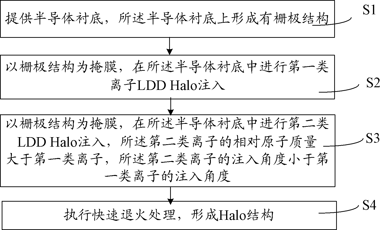
[0025] The method for forming the Halo structure proposed by the present invention will be further described in detail below in conjunction with the accompanying drawings and specific embodiments. Advantages and features of the present invention will be apparent from the following description and claims. It should be noted that all the drawings are in very simplified form, and are only used for the purpose of conveniently and clearly assisting in describing the embodiments of the present invention.

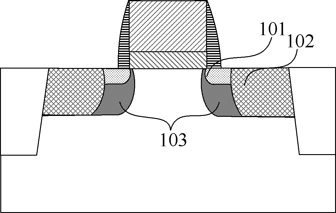
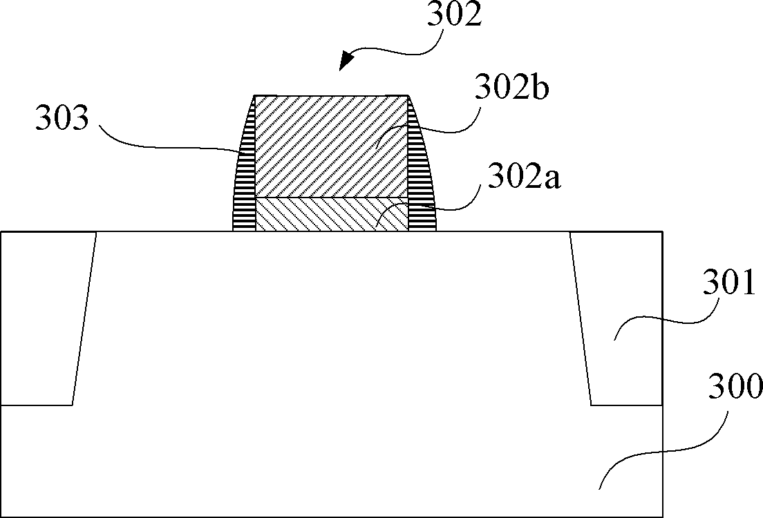
[0026] Such as figure 2 As shown, the present invention provides a method for forming a Halo structure, which is completed by the steps shown in S1 to S4, combined below figure 2 The process flow diagram shown and Figure 3A ~ 3E The schematic diagram of the cross-sectional structure is described in detail for the formation method of the above-mentioned Halo structure.

[0027] S1. A semiconductor substrate is provided, and a gate structure is formed on the semiconductor subs...


PUM


Abstract

The invention provides a formation method of a Halo structure. The method can be used to form an ultra-shallow junction MOS device of a technology node with 65nm and below the 65nm. First kind of ion LDD Halo injection of a wide angle inclination mode and second kind of ion LDD Halo injection of a small angle inclination mode are combined so as to replace traditional phosphorus ion LDD Halo injection. Therefore, threshold shift is effectively reduced; junction capacitance and junction leakage can be effectively reduced too; SCE and DIBI effects are inhibited and an electrical property of the MOS device is increased.

Description

technical field [0001] The invention relates to the field of semiconductor manufacturing, in particular to a method for forming a Halo structure. Background technique [0002] As the size of MOSFET devices continues to shrink, especially when entering the node of 65 nanometers and below, MOSFET devices highlight various unfavorable physical effects due to the extremely short channel, such as short channel effect (SCE), drain-induced barrier lowering effect (DIBL), carrier effect (HCE), source-drain punchthrough, etc., which seriously restrict the improvement of device performance. Among them, SCE determines the channel length and threshold voltage of the device that can be used, which degrades the performance and reliability of the device and limits the further reduction of the feature size. As the feature size of the device reaches 65nm, an ultra-shallow junction structure (a doped junction with a junction depth below 100nm, USJ) is usually used to improve the SCE effect o...

Claims


Application Information

Patent Timeline
IPC IPC(8): H01L21/265H01L21/336
Inventor 赵猛
Owner SEMICON MFG INT (SHANGHAI) CORP
Why Eureka
Try Eureka