Amorphous silicon passivation N-type back contact battery and manufacturing method thereof

A technology of back contact battery and amorphous silicon, which is applied in the direction of circuits, photovoltaic power generation, electrical components, etc., can solve the problems of complicated process and high cost of back junction and back battery, and achieve the advantages of simple process, improved passivation effect, and improved short-circuit current Effect

Inactive Publication Date: 2012-10-17
TRINA SOLAR CO LTD
View PDF3 Cites 8 Cited by
  • Summary
  • Abstract
  • Description
  • Claims
  • Application Information

AI Technical Summary

Problems solved by technology

[0003] The technical problem to be solved by the present invention is: to overcome the deficiencies of the prior art, provide an amorphous silicon passivated back contact battery and its preparation method, and solve the technical problems of high cost and complicated process in the back junction back battery technology

Method used


Image

  • Amorphous silicon passivation N-type back contact battery and manufacturing method thereof

Examples


Embodiment Construction

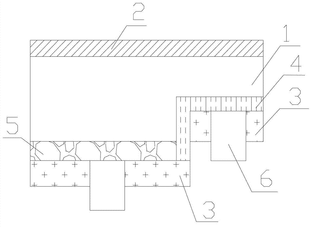
[0026] The present invention is described in further detail now in conjunction with accompanying drawing. These drawings are all simplified schematic diagrams, which only illustrate the basic structure of the present invention in a schematic manner, so they only show the configurations related to the present invention.

[0027] Such as figure 1 A kind of amorphous silicon passivation N-type back contact cell shown, comprises N-type silicon substrate 1, has the P-type doped layer 5 that forms P-type emitter and forms N-type silicon substrate 1 on the back side of N-type silicon substrate 1. For the N-type amorphous silicon layer 4 of the back field, electrodes are formed on the P-type doped layer 5 and the N-type amorphous silicon layer 4 .

[0028] In order to reduce the reflectivity of light, increase the short-circuit current, increase the area of ​​the PN junction, and finally improve the photoelectric conversion efficiency of the cell, both the P-type doped layer 5 and th...


PUM

PropertyMeasurementUnit
thicknessaaaaaaaaaa
reflectanceaaaaaaaaaa

Abstract

The invention relates to an amorphous silicon passivation N-type back contact battery and a manufacturing method thereof. The battery comprises an N-type silicon wafer substrate, a P-type doping layer and an N-type amorphous silicon layer are arranged on the back of the N-type silicon wafer substrate, and electrodes are arranged on the P-type doping layer and the N-type amorphous silicon layer. The manufacturing method of the battery comprises steps of forming the P-type doping layer on the back of the N-type silicon wafer substrate in a diffusion manner through a mask mode; forming a groove in the back of a diffused silicon wafer; and depositing the N-type amorphous silicon layer in the groove through a mask mode. The P-type doping layer and the N-type amorphous silicon layer form a P-type emitting electrode and an N-type back field on the back of the back contact battery, and the electrodes are arranged on the P-type emitting electrode and the N-type back field. The N-type amorphous silicon layer is formed by the silicon wafer, an electric field in the back contact battery is formed by utilizing a good hydrogen passivation effect and a good field passivation effect of the N-type amorphous silicon layer, a passivation effect is improved, the efficiency of the battery is improved obviously, a process is simple, and production efficiency is improved.

Description

technical field [0001] The invention relates to an amorphous silicon passivation N-type back contact battery and a preparation method thereof. Background technique [0002] With the continuous development of the photovoltaic industry, reducing the cost of power generation is a problem that has to be faced, and improving the efficiency of cells is a key measure to reduce costs. Back-junction back-contact battery (BJBC) has all the metal electrodes on the back, and there is no grid line on the front, so the short-circuit current is significantly improved, and the battery efficiency can reach up to 24.2%. Due to the special structure of the BJBC battery, the component cost is further reduced. Contents of the invention [0003] The technical problem to be solved by the present invention is: to overcome the deficiencies of the prior art, provide an amorphous silicon passivated back contact battery and its preparation method, and solve the technical problems of high cost and co...

Claims


Application Information

Patent Timeline
Patent Type & Authority Applications(China)
IPC IPC(8): H01L31/068H01L31/0352H01L31/0224H01L31/18
CPCH01L31/0682H01L31/0747Y02E10/547H01L31/022441
Inventor 陈艳
Owner TRINA SOLAR CO LTD
Why Eureka
Try Eureka