Method for producing plasma display panel
A technology of a display panel and a manufacturing method, which is applied to the manufacture of alternating current plasma display panels, discharge tubes/lamps, cold cathode manufacture, etc. problems with applied voltage
- Summary
- Abstract
- Description
- Claims
- Application Information
AI Technical Summary
Problems solved by technology
Method used
Image
Examples
Embodiment approach
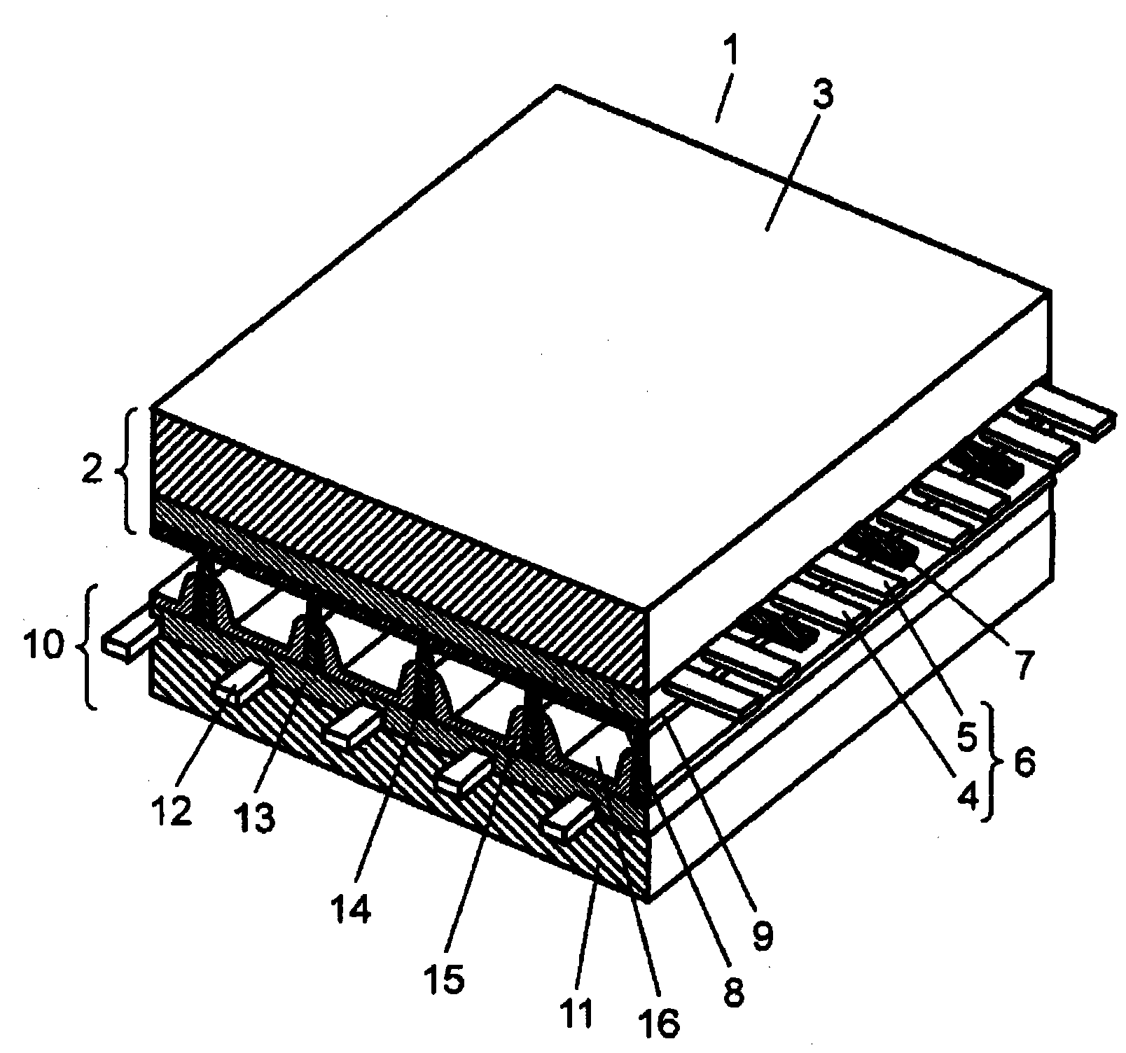
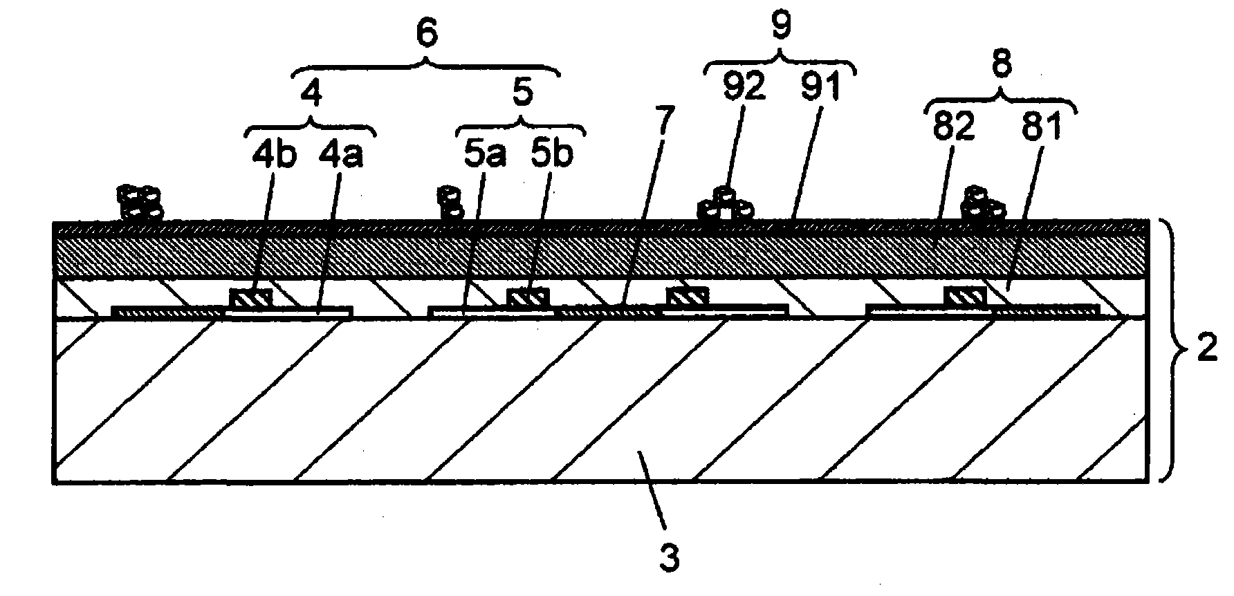
[0047] figure 1 It is a perspective view showing the structure of the PDP 1 manufactured according to the PDP manufacturing method in the embodiment of the present invention. The front panel 2 composed of the front glass substrate 3 and the like and the back panel 10 composed of the back glass substrate 11 and the like are arranged to face each other, and the outer periphery is hermetically sealed by a sealing material composed of glass frit or the like. Discharge gases such as neon (Ne) and xenon (Xe) are enclosed in the discharge space 16 inside the PDP 1 at a pressure of 53.3 kPa to 80.0 kPa. On the front glass substrate 3 of the front panel 2, a pair of strip-shaped display electrodes 6 and black stripes (light-shielding layers) 7 composed of scan electrodes 4 and sustain electrodes 5 are arranged in parallel rows. A dielectric layer 8 that functions as a capacitor is formed on the front glass substrate 3 so as to cover the display electrodes 6 and the light shielding layer...
PUM
| Property | Measurement | Unit |
|---|---|---|
| Thickness | aaaaa | aaaaa |
Abstract
Description
Claims
Application Information


