Method for machining adhesion belt and wafer

A technology of wafer processing and adhesive tape, which is applied in the field of adhesive tape, can solve problems such as device quality degradation and device function damage, and achieve the effect of eliminating quality reduction and suppressing static electricity

Inactive Publication Date: 2012-10-24
DISCO CORP
View PDF5 Cites 4 Cited by
  • Summary
  • Abstract
  • Description
  • Claims
  • Application Information

AI Technical Summary

Problems solved by technology

[0011] However, when the wafer is broken using an expanding device (separating device), the adhesive tape affixed to the wafer expands in the radial direction and an external force is applied to the wafer. Therefore, when the adhesive tape expands, static electricity is generated on the adhesive tape due to friction between the adhesive tape and the expanding device. , there is a problem that the function of the device is destroyed, or the debris when the wafer is disconnected adheres to the device and degrades the quality of the device

Method used


Image

  • Method for machining adhesion belt and wafer
  • Method for machining adhesion belt and wafer
  • Method for machining adhesion belt and wafer

Examples


Embodiment 1

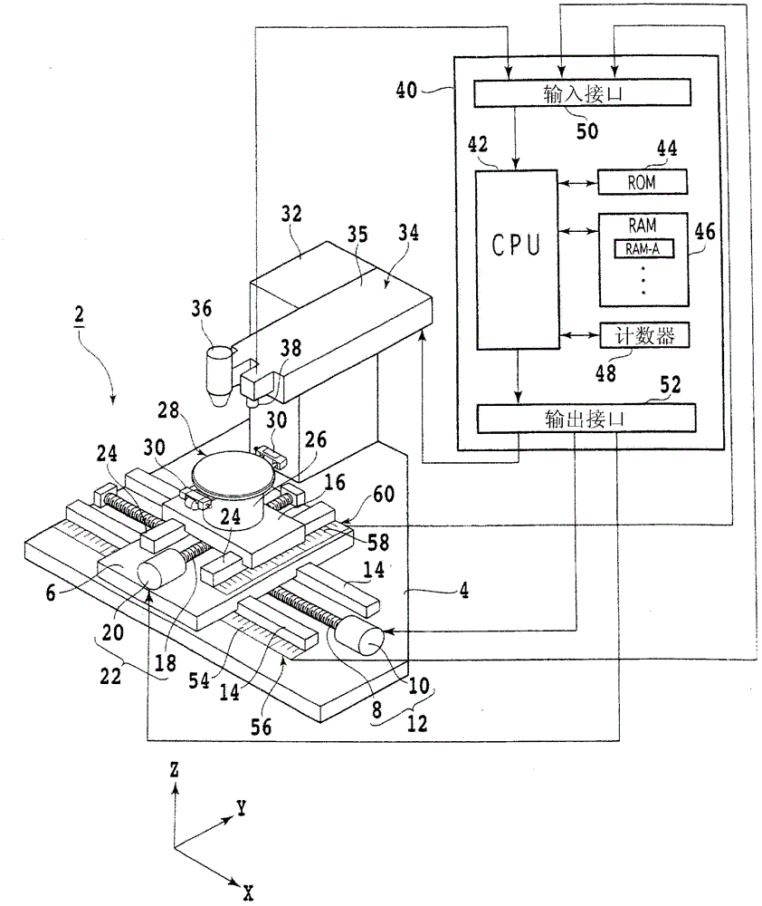
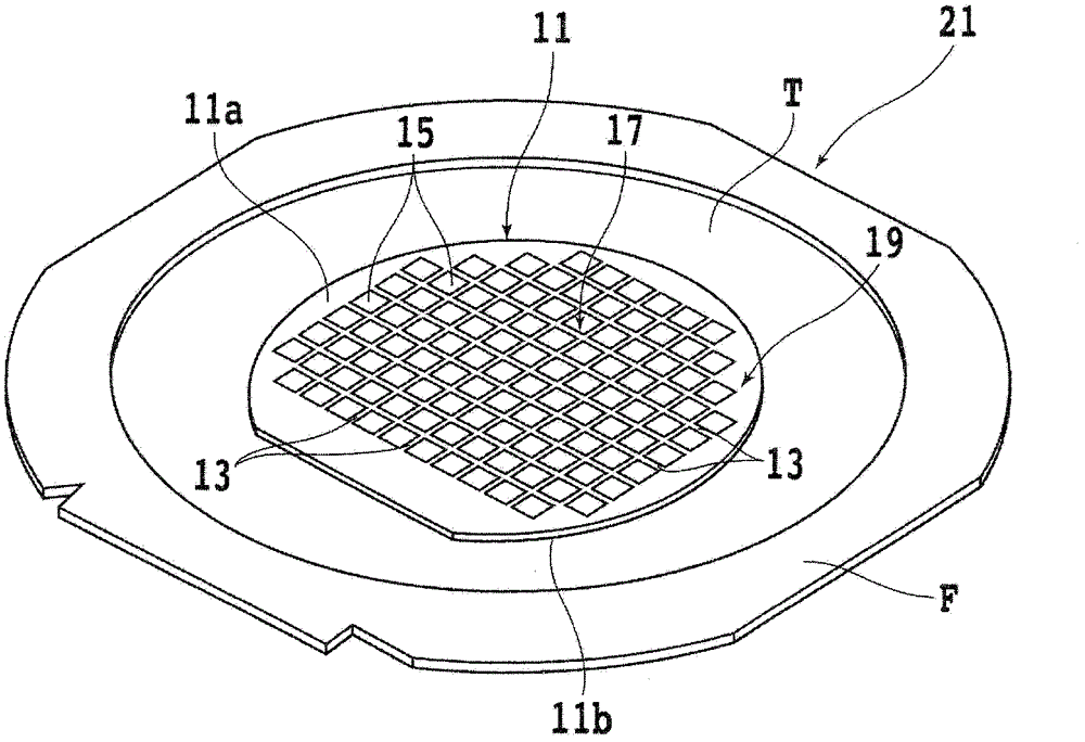
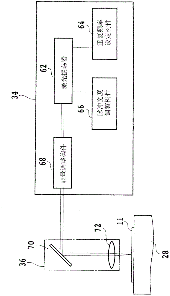
[0087] Such as figure 2 As shown, the silicon wafer 11 is supported by a ring frame F with a dicing tape T interposed therebetween, a laser beam is irradiated at intervals of 1.0 mm to form a degenerated layer inside the planned division line, and a plurality of squares of 1.0 mm×1.0 mm are divided, and then Dilated cutting zone T. The back surface of the dicing tape T was rubbed, and the charge amount of the wafer 11 was compared with the number of debris having a size of 5 μm or more scattered and attached to the surrounding area. The results shown in Table 1 were obtained.

[0088] 【Table 1】

[0089]

[0090] As can be seen from Table 1, the adhesive tape of the present invention having an antistatic layer on the back of the dicing tape T significantly reduced the amount of charge on the wafer compared to the conventional adhesive tape without an antistatic layer. Furthermore, the number of debris on the surface of the chip and the number of debris on the surface of t...


PUM

PropertyMeasurementUnit
thicknessaaaaaaaaaa
diameteraaaaaaaaaa

Abstract

The present invention provides a method for machining an adhesion belt and a wafer using the adhesion belt, wherein the adhesion belt can inhibit static electricity, and is used for supporting the wafer, and the wafer forms a plurality of devices in a manner of being divided by a predetermined separation line on the surface of the wafer, and the wafer is characterized by comprising an adhesion layer laminated on the surface of the thin sheet shaped substrate, and an anti-electrification layer laminated at the back side of the thin sheet shaped substrate.

Description

technical field [0001] The present invention relates to an adhesive tape used when external force is applied to a wafer and a wafer processing method using the adhesive tape. Background technique [0002] Chips such as silicon wafers and sapphire wafers have IC (Integrated Circuit: Integrated Circuit), LSI (Large Scale Integration: Large Scale Integrated Circuit), LED (Light-Emitting Diode: Light-Emitting Diode) and other devices formed on the surface and are scheduled by division. The wafer is divided by a line, and the wafer is divided into individual devices by a processing device, and the divided devices are widely used in various electrical equipment such as mobile phones and personal computers. [0003] A dicing method using a cutting device called a dicer is widely used to divide a wafer. In the dicing method, the wafer is divided into individual devices by cutting the wafer while rotating at a high speed of about 30,000 rpm while cutting the wafer into individual de...

Claims


Application Information

Patent Timeline
Patent Type & Authority Applications(China)
IPC IPC(8): C09J7/02H01L21/683H01L21/78B23K26/36C09J7/20C09J7/24C09J201/00H01L21/301
Inventor 汤平泰吉
Owner DISCO CORP
Why Eureka
Try Eureka