

Transistor and forming method thereof
A transistor and semiconductor technology, applied in semiconductor devices, semiconductor/solid-state device manufacturing, electrical components, etc., can solve problems such as poor performance, achieve better performance, reduce time, and improve performance.
- Summary
- Abstract
- Description
- Claims
- Application Information
AI Technical Summary
Problems solved by technology
Method used
Image

Examples
Embodiment Construction
[0047] As mentioned in the background, existing trench metal-oxide-semiconductor field effect transistors have poor performance.
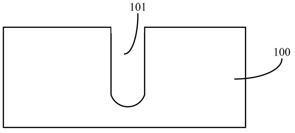
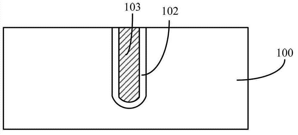
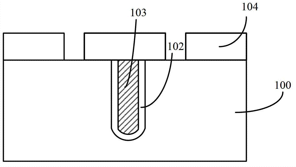
[0048] The inventor of the present invention finds through research, please refer to Figure 5 , in the prior art, after forming the mask layer 104, a conductive plug 106 (such as Figure 4 ) before, using the mask layer 104 as a mask, ion implantation is performed on the semiconductor substrate 100 on both sides of the trench, and thermal annealing is performed to activate the implanted ions to form a source region 105; however, after thermal annealing When the implanted ions are activated, the horizontal diffusion rate of the ions is lower than the vertical diffusion rate; specifically, the lateral diffusion rate of the dopant ions is 60-80% of the vertical diffusion rate; therefore, in order to make the formed source region 105 and gate The contact between the dielectric layer 102 will make the thermal annealing time longer, resulting in the di...
PUM
 Abstract
Description
Claims
Application Information