Method for manufacturing wafer-level light-emitting diode (LED)

A technology of a light-emitting diode and a manufacturing method, which is applied to electrical components, circuits, semiconductor devices, etc., can solve the problems of waste of manufacturing cost, insufficient concentration of color temperature distribution, and inability to manufacture white LEDs with a variety of specific color temperatures. The effect of reducing production costs and solving commercial inventory pressure

Active Publication Date: 2015-05-20
XIAMEN FRIENDLY LIGHTING TECHNOLOGY CO LTD
View PDF5 Cites 0 Cited by
  • Summary
  • Abstract
  • Description
  • Claims
  • Application Information

AI Technical Summary

Problems solved by technology

[0004] In the prior art, the spray method is often used to obtain a uniform phosphor film. However, this method is easy to manufacture white LEDs at the wafer level due to the brightness and wavelength distribution of the epitaxial chip itself. There is still the problem that the color temperature distribution is not concentrated enough
[0005] In addition, the existing method of spraying phosphor powder can only spray the phosphor powder on the wafer all at once, resulting in white LEDs that can only be fixed at a specific color temperature and cannot be fabricated on a single wafer White LEDs that can form a variety of specific color temperatures
[0006] Moreover, blue light crystal grains that cause wavelength shift after being coated with fluorescent powder cannot continue to be sold to manufacturers that need blue light grains. This not only creates inventory pressure for commercial use, but also causes waste of production costs.

Method used


Image

  • Method for manufacturing wafer-level light-emitting diode (LED)
  • Method for manufacturing wafer-level light-emitting diode (LED)
  • Method for manufacturing wafer-level light-emitting diode (LED)

Examples


Embodiment Construction

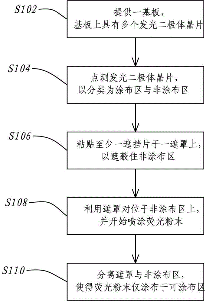
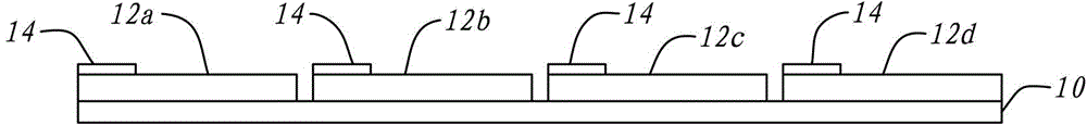
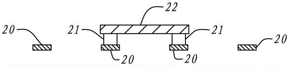
[0041] The present invention proposes a wafer-level light-emitting diode manufacturing method, which uses shielding and shielding sheets to cover the crystal grains that do not need to be sprayed, so as to achieve the purpose of partially spraying fluorescent powder on the crystal grains whose brightness and wavelength meet the requirements.

[0042] When the process method of the present invention is repeated, white light emitting diodes with different specific color temperatures can be fabricated on a single wafer (or substrate) according to the photoelectric characteristic requirements of different crystal grains.

[0043] Please refer to figure 1 , is a flow chart of steps of a method for manufacturing a wafer-level light-emitting diode according to an embodiment of the present invention. The method includes steps S102, S104, S106, S108, and S110. The following is to explain the technical idea of ​​the present invention, please refer to Figure 2 to Figure 6 shown.

[00...


PUM


Abstract

The invention discloses a method for manufacturing a wafer-level light-emitting diode (LED). The method comprises the following steps of: providing a substrate, wherein a plurality of LED chips are arranged on the substrate; performing spot measurement on the LED chips, so that the LED chips are classified into a coating region and a non-coating region; pasting at least one shielding piece on a shield, so that the non-coating region in the LED chips is shielded; aligning the shield on the non-coating region, and spraying fluorescent powder; and separating the shield from the non-coating region, so that the fluorescent powder is only sprayed in the coating region in the LED chips. According to the manufacturing method, the limitation that the known fluorescent powder needs to be sprayed in the whole wafer can be avoided, and a white LED with different color temperature requirements can be manufactured on a single wafer.

Description

technical field [0001] The invention relates to a method for manufacturing a wafer-level light-emitting diode, in particular to a method for making a white light-emitting diode with uniform color temperature by partially spraying fluorescent powder. Background technique [0002] With the great improvement of epitaxy, manufacturing process and packaging technology, the Light emitting diode (LED) of inorganic materials has surpassed the traditional application scope. Internal and external warning lighting, large outdoor billboards, etc.; in the general lighting part, LEDs are gradually developing from the current auxiliary lighting purpose to an important main lighting source. [0003] Generally speaking, white light LEDs made of phosphor powder excited by blue light grains are widely used in the market due to their advantages of simple driving circuit and low cost. However, its disadvantages also include: the conversion efficiency of phosphor is poor, the light emission inte...

Claims


Application Information

Patent Timeline
Patent Type & Authority Patents(China)
IPC IPC(8): H01L33/50B05D1/32
Inventor 张源孝
Owner XIAMEN FRIENDLY LIGHTING TECHNOLOGY CO LTD
Why Eureka
Try Eureka