Metal printed circuit board having aperture reflection plane and manufacturing method

A technology of printed circuit boards and manufacturing methods, which is applied in the direction of printed circuit manufacturing, printed circuits, printed circuits, etc., can solve problems such as uneven structure, additional manufacturing costs, and influence on color temperature, so as to improve reflection efficiency, reduce costs, and prevent diffusion Effect

Inactive Publication Date: 2012-11-28
斗星A-TECH +1
View PDF4 Cites 0 Cited by
  • Summary
  • Abstract
  • Description
  • Claims
  • Application Information

AI Technical Summary

Problems solved by technology

In this case, not only additional manufacturing costs are required, but also the color temperature is affected due to the uneven structure of the dam.

Method used


Image

  • Metal printed circuit board having aperture reflection plane and manufacturing method
  • Metal printed circuit board having aperture reflection plane and manufacturing method
  • Metal printed circuit board having aperture reflection plane and manufacturing method

Examples


Embodiment Construction

[0055] The following describes in detail a preferred embodiment of the metal printed circuit board with a reflective surface with holes and its manufacturing method according to the present invention.

[0056] Through the detailed description of the following embodiments, the characteristics and advantages of the metal printed circuit board with a reflective surface with holes and its manufacturing method according to the present invention will be more clarified.

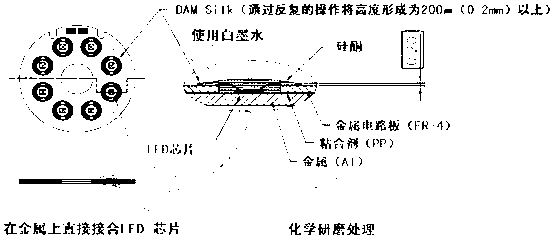
[0057] Figure 2a to Figure 2g It is a cross-sectional view of the manufacturing process of a metal printed circuit board with a hole reflecting surface according to the present invention.

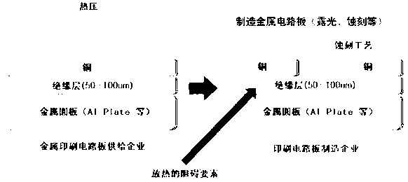
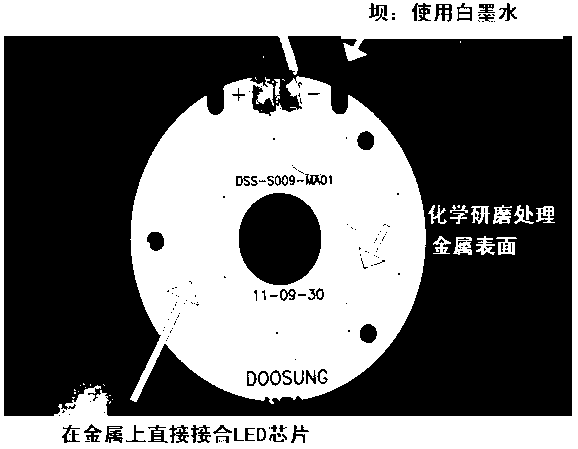
[0058] In the present invention, the process of forming the primary reflective structure is formed by processing the surface of the metal circular plate by processes such as chemical polishing, rather than by expensive processes such as gold plating. In the process of forming the secondary reflective structure, the reflective surface i...


PUM


Abstract

The invention relates to a metal printed circuit board having an aperture reflection plane and the manufacturing method thereof, wherein a technology for forming the reflection plane through the surface processing of a metal circular plate and a jointing technolgy for forming a perforated printed circuit board (PCB) are carried out through a single technology, thereby improving the simplificaiton of the manufaturing technology and the usability of products. The metal printed circuit board includes the metal circular plate which is provided with a primary refleciton plane formed at a chip jointing area through the surface processing; a PCB layer which is laminated on the metal circular plate and is provided with an aperture and a wiring pattern formed on the chip jointing area; a secondary reflection plane formed on the inner side surface of the holes of the PCB layer, and a dam which is formed on the PCB board surrounding the hole by taking the hole as the center.

Description

Technical field [0001] The invention relates to a metal printed circuit board (PCB, Printed Circuit Board). More specifically, it relates to a metal printed circuit board with a hole reflecting surface and a method of manufacturing the same, in which the process of forming the reflecting surface by the surface treatment of the metal disc and the bonding process of the printed circuit board forming the hole are performed in a single process, This improves the simplification of the manufacturing process and the usability of the product. Background technique [0002] Generally, a light emitting diode (LED), as a component that emits light when electrons and holes (Positive Hole) meet at a P-N junction (P-N junction) according to the introduced current, is usually fabricated into a package structure carrying an LED chip. [0003] Such an LED package is generally formed such that it is provided on a printed circuit board, and current is drawn in from an electrode formed on the printed ...

Claims


Application Information

Patent Timeline
Patent Type & Authority Applications(China)
IPC IPC(8): H05K1/02H05K1/18H05K3/00H01L33/62H01L33/60
CPCH05K2201/09027H05K2201/2054H05K1/02F21V29/00H05K3/00H01L25/075H05K2201/10106H05K1/18H05K3/0061H01L33/62F21S4/00H01L33/60H01L33/64H01L2224/48091H01L2224/48227Y10T29/49124H01L2924/00014
Inventor 张种镇
Owner 斗星A-TECH
Why Eureka
Try Eureka