Photoetching layout, photoresist graph and method for measuring exposure error of photoresist graph

A photoresist, measuring light technology, applied in microlithography exposure equipment, photolithography process exposure devices, originals for photomechanical processing, etc., can solve the problems of complex process and long test time, and simplify the test steps , the effect of saving test time

Active Publication Date: 2012-12-05
SHANGHAI HUAHONG GRACE SEMICON MFG CORP
View PDF5 Cites 13 Cited by
  • Summary
  • Abstract
  • Description
  • Claims
  • Application Information

AI Technical Summary

Problems solved by technology

[0006] However, when measuring the exposure error between different unit regions on the same layer of photoresist in the prior art, at least ...

Method used


Image

  • Photoetching layout, photoresist graph and method for measuring exposure error of photoresist graph
  • Photoetching layout, photoresist graph and method for measuring exposure error of photoresist graph
  • Photoetching layout, photoresist graph and method for measuring exposure error of photoresist graph

Examples


no. 1 example

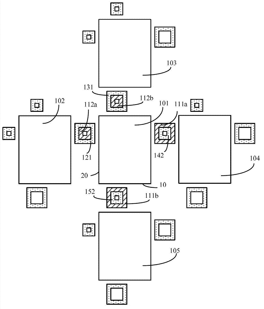
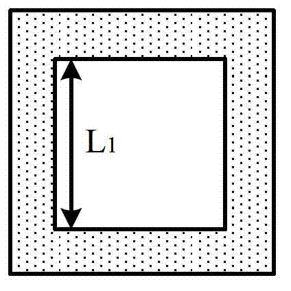
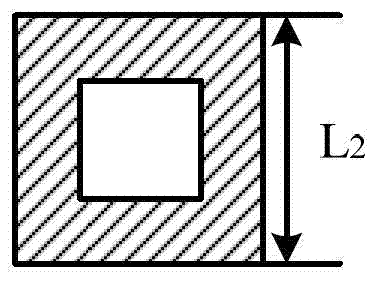
[0055] Please refer to Figure 5 , is a schematic diagram of the first embodiment of the lithographic layout of the present invention, including: a first unit area pattern 201, the first unit area pattern 201 is rectangular; four corners of the first unit area pattern 201 The first mark graphic 211a, the first mark figure 211b, the first mark figure 211c, the first mark figure 211d on the outside, the first mark figure 211a, the first mark figure 211b, the first mark figure 211c, the first mark figure 211d are all "L" shapes, and the two sides of the "L" shape are respectively parallel to the adjacent two sides constituting the top corner of the first unit area figure 201; The second marking figure 212 outside the first marking figure 211a, the second marking figure 212 is in the shape of a "ten", and the two sides forming the "ten" shape are respectively parallel to the two sides of the corresponding first marking figure 211a.

[0056] The region of the first unit area patte...

no. 2 example

[0062] Please refer to Image 6 , is a schematic diagram of the second embodiment of the photoresist pattern of the present invention, including:

[0063] The first unit area 301, the first unit area 301 is rectangular; the first mark 311a, the first mark 311b, the first mark 311c and the first mark 311d located outside the four corners of the first unit area 301, The first mark 311a, the first mark 311b, the first mark 311c and the first mark 311d are all in the shape of an "L", and the two sides of the "L" shape are respectively connected to the corners of the first unit area 301. The adjacent two sides are parallel; the second mark 312 located at a vertex of the first unit area 301 and outside the first mark 311a, the second mark 312 is a "ten" shape, and the two sides constituting the "ten" shape are respectively parallel to the two sides of the first mark 311a.

[0064] The second unit area 302, the third unit area 303 and the fourth unit area 304 arranged parallel to t...

no. 3 example

[0072] Correspondingly, the inventors of the present invention also provide a third embodiment of a method for measuring exposure errors of photoresist patterns, please refer to Figure 7 with Figure 8 , Figure 7 is the photoresist pattern used to measure the exposure error in this embodiment, Figure 8 yes Figure 7 An enlarged view of the middle area 400 .

[0073] Please refer to Figure 5 , provide a photoresist pattern, the photoresist pattern includes: a first unit area 401, a second unit area 402, a third unit area 403 and a fourth unit area 404, the first unit area 401, the second unit area Adjacent boundaries of the area 402, the third unit area 403 and the fourth unit area 404 are parallel to each other and constitute a 2×2 array of unit areas; the first unit area 401, the second unit area 402, the third unit area 403 and the Each corner of the fourth unit area 404 has a first mark on the outer side, the first mark is "L" shape, and the two sides of the "L" sh...


PUM

PropertyMeasurementUnit
Widthaaaaaaaaaa

Abstract

The invention discloses a photoetching layout, a photoresist graph and a method for measuring an exposure error of the photoresist graph. The photoetching layout comprises a first die graph, four first mark graphs, and a second mark graph, wherein the first die graph is a rectangle; the four first mark graphs are positioned on the outer sides of four top corners of the first die graph, and have L shapes; two edges of each L shape are respectively parallel to two adjacent edges which form one top corner of the first die graph; the second mark graph is positioned on the outer sides of one top corner of the first die graph and the corresponding first mark graph, and has a cross shape; and two edges forming the cross shape are respectively parallel to the two edges of the corresponding first mark graph. In the process of forming the photoresist graph by using the photoetching layout, the exposure error between two times of exposure on the same photoresist layer can be acquired through one-time measurement, so that measuring steps are reduced, and testing time is saved.

Description

technical field [0001] The invention relates to the technical field of semiconductor manufacturing, in particular to a photolithography layout, a photoresist pattern and a method for measuring the exposure error of the photoresist pattern. Background technique [0002] In the existing semiconductor manufacturing process, before semiconductor devices are fabricated on the wafer, the wafer needs to be layout designed, and the wafer is divided into several unit areas (Die) and scribe lanes (Scribe lane) between the unit areas. . Wherein, the unit area is used to subsequently form a semiconductor device, and the dicing line is used as a cutting line when the unit area (Die) is divided in the packaging stage when the semiconductor device is manufactured. [0003] The division of the unit area and the dicing line on the wafer surface is realized by copying the pattern on the mask plate to the wafer surface through a photolithography process. The specific method is: a photoresist ...

Claims


Application Information

Patent Timeline
IPC IPC(8): G03F1/44G03F1/42G03F7/20H01L21/66
Inventor 岳力挽赵新民周孟兴王彩虹
Owner SHANGHAI HUAHONG GRACE SEMICON MFG CORP
Why Eureka
Try Eureka