
A dual-polarized antenna and a mimo antenna with the dual-polarized antenna
A dual-polarized antenna and antenna technology, applied in the field of MIMO antennas, can solve the problems of versatility and performance differences, and achieve the effects of strong anti-interference ability, low broadband multi-mode, and low operating frequency
- Summary
- Abstract
- Description
- Claims
- Application Information
AI Technical Summary
Problems solved by technology
Method used
Image

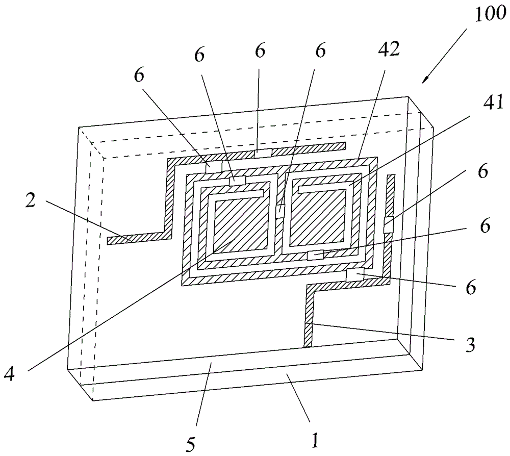
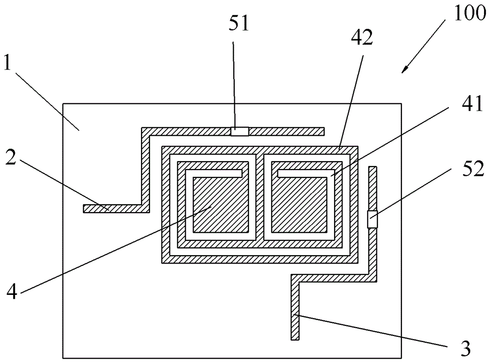
Examples
Embodiment 2
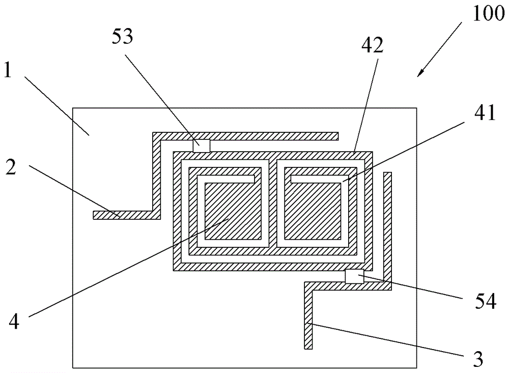
[0045] Such as image 3 As shown, in this embodiment, spaces 53 and 54 for embedding capacitive electronic components are preset between the first feeder 2 and the metal sheet 4, and between the second feeder 3 and the metal sheet 4. The preset embedding The position of the electronic component space can be any position between the first feeder 2 and the metal sheet 4 , and between the second feeder 3 and the metal sheet 4 . image 3 The middle space 53 and the space 54 are spaces for embedding capacitive electronic components in this embodiment. There is a certain capacitance between the first feeder 2, the second feeder 3 and the metal sheet 4. Here, the first feeder 2, the second feeder 3 and the metal sheet 4 are adjusted by embedding capacitive electronic components. The signal coupling between the feeder 2, the second feeder 3 and the metal sheet 4 uses the formula: It can be seen that the capacitance value is inversely proportional to the square of the operating frequ...
Embodiment 3
[0047] Such as Figure 4 As shown, in this embodiment, a space for embedding inductive electronic components and / or resistors is reserved on the metal wiring 42 of the metal sheet, and the space for embedding electronic components is not limited to the space 55 and the space given in the figure 56. Other positions are acceptable as long as the conditions are met. The purpose of embedding inductive electronic components here is to increase the inductance value of the resonant structure inside the metal sheet, thereby adjusting the resonant frequency and working bandwidth of the antenna; same as the first embodiment, the purpose of embedding resistors here is to improve the antenna's radiation resistance. As for embedding inductive electronic components or resistors, it depends on the needs. In addition, wires are used to short-circuit in the space where electronic components are not embedded.
Embodiment 4
[0049] Such as Figure 5 As shown, in this embodiment, a space for embedding capacitive electronic components is reserved on the microgroove structure 41 , and the space connects the metal wires 42 on both sides of the microgroove structure 41 . The space for embedding electronic components is not limited only to the Figure 5 The space 57 given in , other locations are all available as long as the conditions are met. Embedding capacitive electronic components can change the resonance performance of the metal sheet, and ultimately improve the Q value and resonance operating point of the antenna. As common knowledge, we know that the relationship between the passband BW, the resonant frequency w0 and the quality factor Q is: BW=wo / Q, this formula shows that the larger Q is, the narrower the passband is, and the smaller Q is, the wider the passband is. In addition: Q=wL / R=1 / wRC, wherein, Q is the quality factor; w is the power frequency when the circuit resonates; L is the ind...
PUM
 Abstract
Description
Claims
Application Information