Gate driver
一种栅极驱动电路、栅极的技术,应用在电气元件、电子开关、高效电力电子转换等方向,能够解决误动作、变低等问题,达到稳定导通的效果
- Summary
- Abstract
- Description
- Claims
- Application Information
AI Technical Summary
Problems solved by technology
Method used
Image
Examples
Embodiment 1
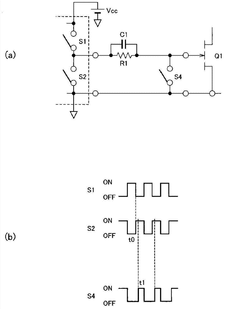
[0032] figure 1 It is a circuit configuration diagram and a sequence diagram of the gate drive circuit according to Embodiment 1 of the present invention. exist figure 1 In the shown gate drive circuit, a series circuit of a switch S1 and a switch S2 is connected to both ends of the power supply Vcc. A pulse signal is generated by turning the switch S1 and the switch S2 on and off alternately. The switch S1 and the switch S2 correspond to a control circuit, and the pulse signal corresponds to a control signal.
[0033] The switching element Q1 is formed of a GaNFET and has a gate, a drain, and a source. A CR parallel circuit of a capacitor C1 and a resistor R1 is connected between the gate of the switching element Q1 and the connection point of the switches S1 and S2.
[0034] The aforementioned pulse signal is applied to the gate of the switching element Q1 via a CR parallel circuit of the capacitor C1 and the resistor R1.
[0035] In addition, in the gate drive circui...
Embodiment 2
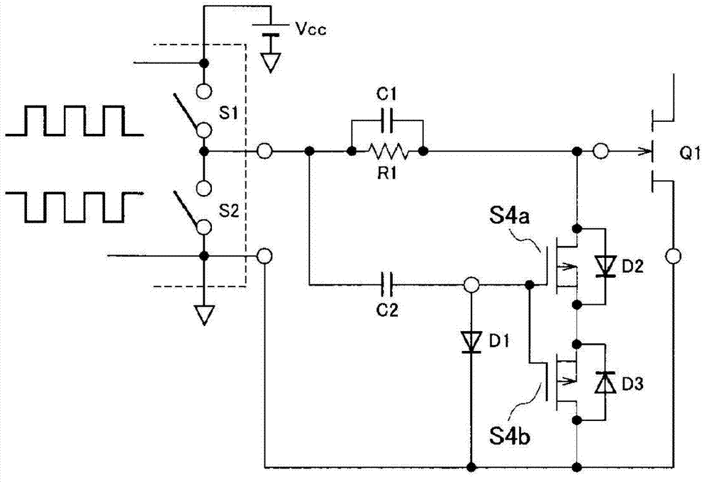
[0043] figure 2 It is a circuit configuration diagram of the gate drive circuit of the second embodiment. figure 2 In the illustrated second embodiment, the switch S4 is constituted by bidirectional switches S4a and S4b that connect the sources and gates of n-type MOSFETs or p-type MOSFETs in common, respectively. The bidirectional switches S4a, S4b are connected in parallel to the gate / source of the switching element Q1. After the switching element Q1 is turned off, when a signal for turning on the bidirectional switches S4a and S4b is applied after a certain period of time has elapsed, the discharge of the capacitor C1 in the CR parallel circuit is quickly terminated. During the regenerative operation, it is preferable that the bidirectional switches S4a and S4b remain in the on state during the off period of the switching element Q1.
[0044] When a conventional gate driver IC is used, it is very troublesome to generate a signal for controlling the switch S4. When a p-...
Embodiment 3
[0056] Figure 4 It is a circuit configuration diagram of the gate drive circuit of the third embodiment. exist Figure 4 In the illustrated third embodiment, a capacitor C2 is connected between the gates of the bidirectional switches S4a, S4b and the output of the driver IC. A series circuit of a diode D1 and a resistor R2 is connected between the gates of the bidirectional switches S4a, S4b and the gate of the switching element Q1.
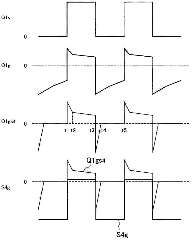
[0057] According to this configuration, at the instant when switching element Q1 is turned off, a negative voltage is applied to switching element Q1 due to the effect of the CR parallel circuit. Based on the time constant of the resistor R2 and the capacitor C2 connected to the gates of the bidirectional switches S4a, S4b, the gate voltage of the bidirectional switches S4a, S4b gradually increases to a negative voltage.
[0058] Furthermore, when the gate voltage of the switching element Q1 is a negative voltage, the switch S4b constituting ...
PUM
 Abstract
Description
Claims
Application Information


