Preparation method of silicon film

A technology of silicon film and silicon substrate, which is applied in the field of semiconductor device preparation, can solve the problems of different corrosion rates, the influence of silicon film uniformity, difficulty in obtaining uniform silicon film with precise thickness, etc., so as to control the degree of corrosion and ensure uniformity and the effect of thickness consistency

Inactive Publication Date: 2012-12-12
WUXI CHINA RESOURCES HUAJING MICROELECTRONICS
View PDF5 Cites 1 Cited by
  • Summary
  • Abstract
  • Description
  • Claims
  • Application Information

AI Technical Summary

Problems solved by technology

As known to those skilled in the art, when the depth of etching is controlled according to time, after the etching operation is stopped, the remaining KOH solution on the silicon wafer 10 will also slightly etch the silicon wafer, resulting in the silicon film 101 There is a certain error in the thickness due to time control, so there is a certain lack of time control in terms of rigor
In addition, there are other problems in this conventional technology: for example, because the thickness of the starting silicon wafer 10 has fluctuations of several microns, the uniformity of the obtained silicon film is greatly affected; if there is an impurity gradient in the silicon wafer or defects, it will also lead to different etching rates in different regions of the silicon wafer, which will also cause the problem of uneven surface and inconsistent thickness of the silicon film; in addition, there are large errors in the measurement of the thickness and etching depth of the silicon wafer
To sum up, it can be seen that although the conventional preparation technique is simple, it is difficult to obtain a uniform silicon film with precise thickness.

Method used


Image

  • Preparation method of silicon film
  • Preparation method of silicon film
  • Preparation method of silicon film

Examples


Embodiment Construction

[0017] Further illustrate the present invention below in conjunction with accompanying drawing. Those skilled in the art can understand that the following only describes the gist of the present invention in conjunction with specific embodiments, and does not limit the implementation of the present invention to this example. The scope of the present invention is determined by the appended claims, and any modifications and changes that do not deviate from the spirit of the present invention shall be covered by the claims of the present invention.

[0018] In the following embodiments, the silicon substrate is single crystal silicon, and the prepared silicon film is described as a thin single crystal silicon film used in MEMS, for example, but it should be understood that this embodiment is illustrative rather than restrictive.

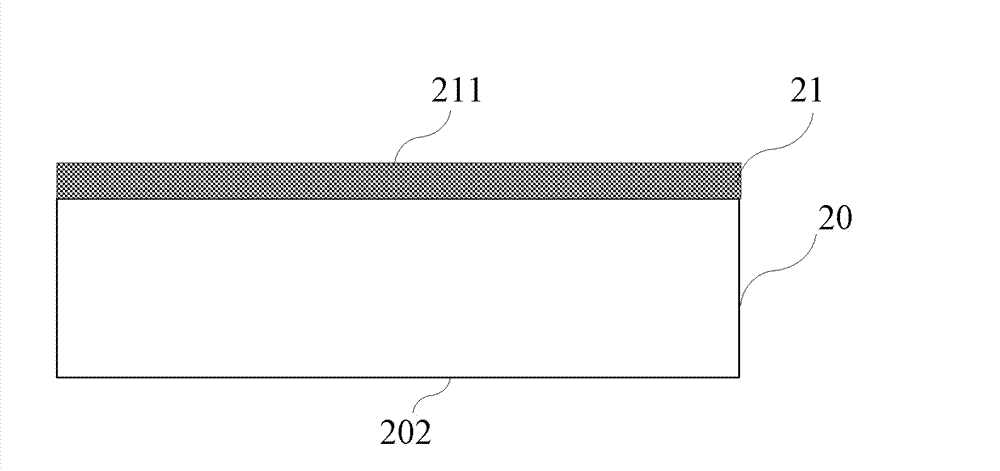
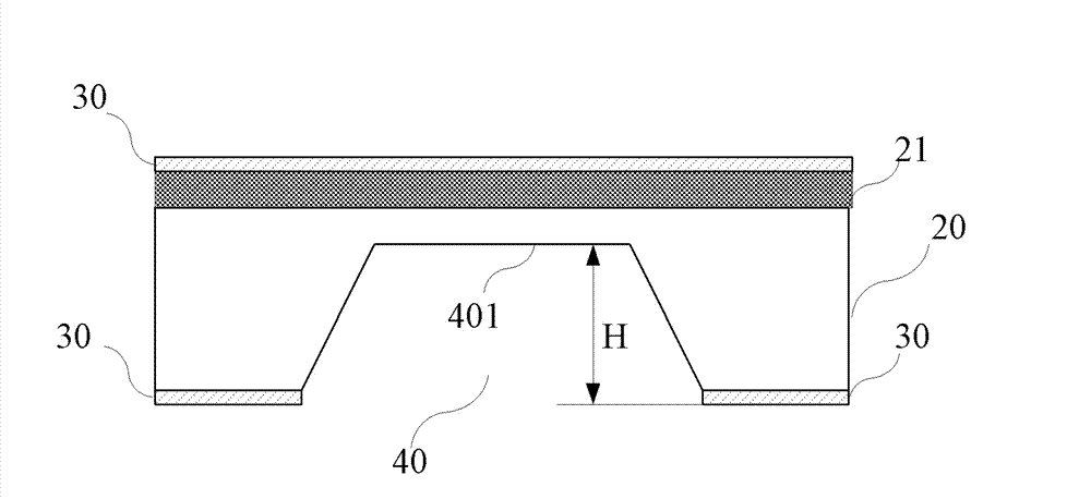
[0019] image 3 Shown is a heavily doped crystal silicon substrate 20 . The dopant in the single crystal silicon substrate 20 can be a conv...


PUM

PropertyMeasurementUnit
electrical resistivityaaaaaaaaaa

Abstract

The invention provides a preparation method of a silicon film. The method comprises the steps that: a heavily doped silicon substrate is formed; a lightly doped silicon film layer is formed by extension on a first surface of the silicon substrate; a first etching liquid is adopted, and a back cavity with a first depth is formed on a second surface of the silicon substrate with an etching method, wherein the second surface is opposite to the first surface; and a second etching liquid is adopted, and the back cavity is corroded until the silicon film layer is exposed. With the method, a uniform silicon film with a consistent thickness can be obtained.

Description

technical field [0001] The invention relates to semiconductor device preparation technology, in particular to the preparation of silicon film. Background technique [0002] Micro-Electro-Mechanical Systems (MEMS) technology is one of the high-tech technologies that have developed rapidly in recent years. Because it adopts advanced semiconductor manufacturing process, it can realize mass production of MEMS. [0003] Silicon membrane is one of the important components of MEMS devices, such as the sensitive membrane of pressure sensors. Correspondingly, the preparation of silicon film is one of the key technologies in the development and application of MEMS devices. For the manufacture of large-scale pressure sensors, the uniformity and consistency of the sensitive film thickness of each sensor is a very critical indicator. To put it simply, the conventional technique for preparing a silicon film is to use an alkaline solution to perform anisotropic etching from ...

Claims


Application Information

Patent Timeline
Patent Type & Authority Applications(China)
IPC IPC(8): B81C1/00
Inventor 王荣华朱琳荆二荣陈思奇
Owner WUXI CHINA RESOURCES HUAJING MICROELECTRONICS
Why Eureka
Try Eureka