Method for detecting film stress distribution

A technology of film stress and detection method, which is applied in the direction of measuring the change force of optical properties of materials when they are stressed, can solve the problems of inability to detect film stress, and achieve the advantages of shortening measurement time, simplifying measurement process and rapid detection. Effect

Inactive Publication Date: 2012-12-12
SHANGHAI HUALI MICROELECTRONICS CORP
View PDF6 Cites 8 Cited by
  • Summary
  • Abstract
  • Description
  • Claims
  • Application Information

AI Technical Summary

Problems solved by technology

[0008] The purpose of the present invention is to solve the problem that the existing curvature radius measurement metho

Method used


Image

  • Method for detecting film stress distribution
  • Method for detecting film stress distribution
  • Method for detecting film stress distribution

Examples


Embodiment Construction

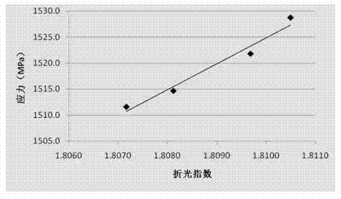
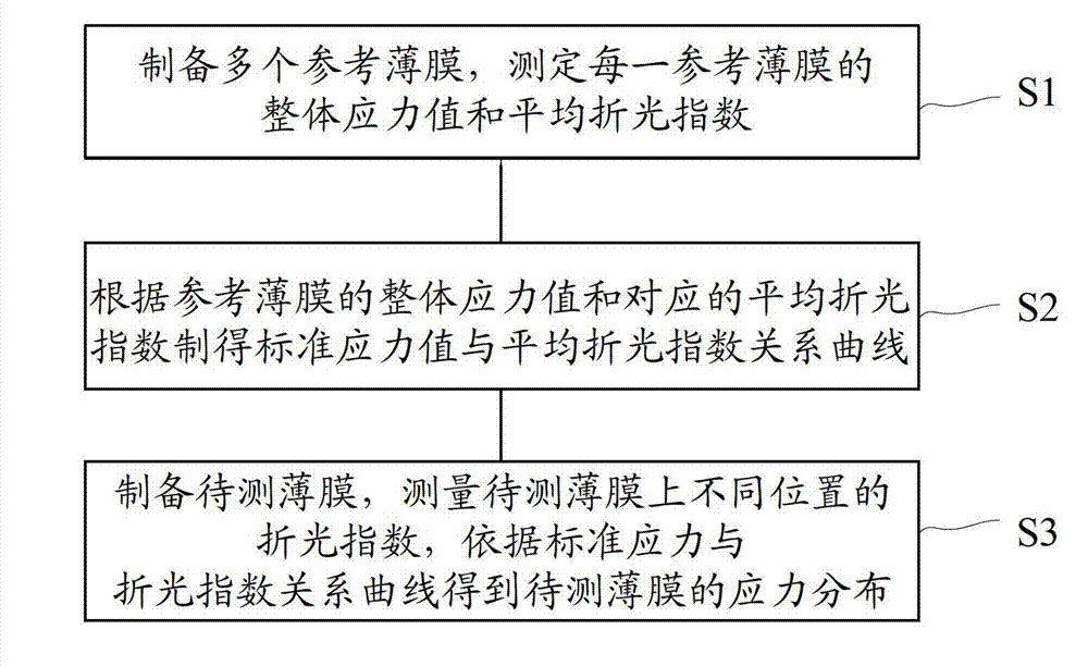
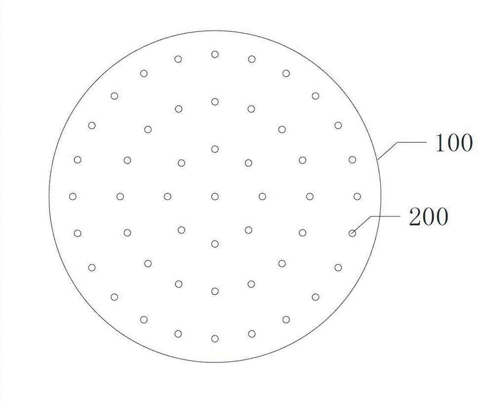
[0030] The detection method of the film stress distribution of the present invention will be described in more detail below in conjunction with the schematic diagram, wherein a preferred embodiment of the present invention is represented, it should be understood that those skilled in the art can modify the present invention described here, and still realize the present invention beneficial effect. Therefore, the following description should be understood as the broad knowledge of those skilled in the art, but not as a limitation of the present invention.

[0031] In the following paragraphs the invention is described more specifically by way of example with reference to the accompanying drawings. Advantages and features of the present invention will be apparent from the following description and claims. It should be noted that all the drawings are in a very simplified form, and are only used for the purpose of conveniently and clearly assisting in describing the embodiments o...


PUM


Abstract

The invention discloses a method for detecting film stress distribution. The method for detecting film stress distribution comprises the following steps: manufacturing a plurality of reference films with different process parameters by using a deposition process; measuring an overall stress value and an average refractive index of each reference film; making a relation curve of a standard stress value and the average refractive index according to the overall stress value and the corresponding average refractive index of the reference film; preparing a film to be measured; measuring the refractive indexes of points to be detected at different positions on the film to be measured; obtaining the stress value of each point to be detected of the film to be measured according to the relation curve of the standard stress value and the average refractive index; and determining the stress distribution of the film to be measured. With the adoption of the method, the stress distribution situation of the film to be measured can be obtained only by measuring the refractive index of the film to be measured for only one time, thereby being beneficial to carrying out detection control over film deposition.

Description

technical field [0001] The invention relates to the technical field of semiconductor devices, in particular to a detection method for film stress distribution. Background technique [0002] In the field of semiconductor device technology, from a macroscopic point of view, the main reason for the stress of the film is the difference in thermal contraction coefficient between the film and the substrate of the semiconductor device. The film has no stress when it is deposited on the substrate of the semiconductor device at a relatively high temperature, but when the film is cooled, due to a certain difference in thermal contraction coefficient between the film and the substrate, it shows a certain stress. [0003] At the same time, the film also has a certain internal stress, which is mainly caused by the lattice defects inside the film material or the distortion energy inside the amorphous material. The film stress is usually the sum of the stress components caused by various f...

Claims


Application Information

Patent Timeline
IPC IPC(8): G01L1/24
Inventor 徐强
Owner SHANGHAI HUALI MICROELECTRONICS CORP
Why Eureka
Try Eureka