Multi-chip packaging structure and multi-chip packaging method

A multi-chip packaging and chip technology, applied in the direction of semiconductor/solid-state device parts, semiconductor devices, electrical components, etc., can solve the problems of large packaging area, complex manufacturing process, high cost, achieve high current parameters, improve reliability, good isolation effect

Active Publication Date: 2012-12-19
HEFEI SMAT TECH CO LTD
View PDF3 Cites 24 Cited by
  • Summary
  • Abstract
  • Description
  • Claims
  • Application Information

AI Technical Summary

Problems solved by technology

[0007] In view of this, the purpose of the present invention is to provide a novel power integrated circuit chip packaging s

Method used


Image

  • Multi-chip packaging structure and multi-chip packaging method
  • Multi-chip packaging structure and multi-chip packaging method
  • Multi-chip packaging structure and multi-chip packaging method

Examples


Embodiment Construction

[0039] Several preferred embodiments of the present invention will be described in detail below with reference to the accompanying drawings, but the present invention is not limited to these embodiments. The present invention covers any alternatives, modifications, equivalent methods and schemes made on the spirit and scope of the present invention. In order to provide the public with a thorough understanding of the present invention, specific details are set forth in the following preferred embodiments of the present invention, but those skilled in the art can fully understand the present invention without the description of these details.

[0040]The multi-chip packaging structure according to the present invention will be described in detail below in conjunction with specific embodiments.

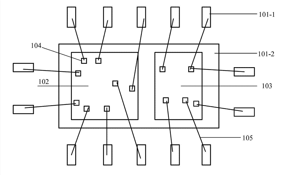
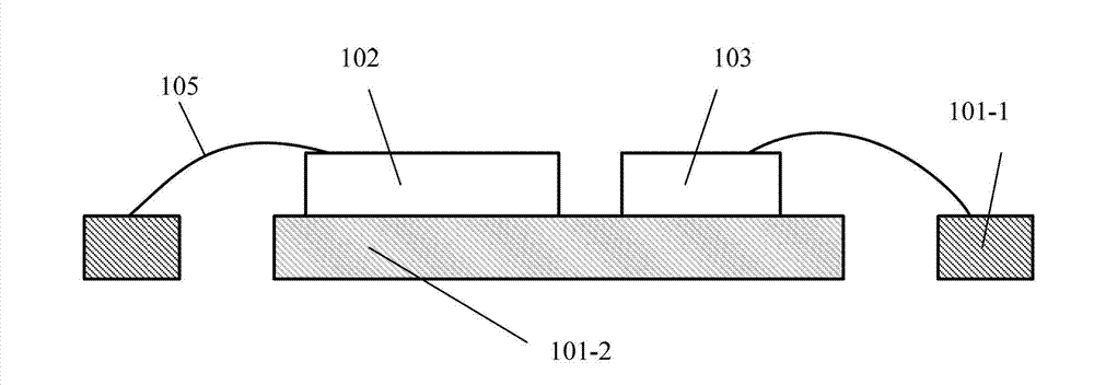
[0041] refer to Figure 3A , showing a top view of a multi-chip packaging structure according to an embodiment of the present invention, and Figure 3B shown Figure 3A A cross-sectio...


PUM


Abstract

The embodiment of the invention provides a multi-chip packaging structure and a multi-chip packaging method. n chips are sequentially stacked and arrayed on a chip loading platform; moreover, each chip partially covers the chip of the lower layer, so that a pad of the chip of the lower layer is exposed; a second bonding lead connects the pad on one chip to the pad on the other chip; and a first bonding lead connects the pad to a pin, accordingly, a minimum packaging area is obtained, moreover, the lengths of the first bonding lead and the second bonding lead are shortest, the powder loss which is caused by the self resistances of the bonding leads is lowered, and the reliability of the lead bonding is improved.

Description

technical field [0001] The invention relates to the field of integrated circuits, and more specifically relates to a multi-chip packaging structure and a packaging method thereof. Background technique [0002] In the semiconductor industry, the production of integrated circuits can be divided into three stages: integrated circuit design, integrated circuit manufacturing and integrated circuit packaging. In the manufacture of integrated circuits, chips are completed by the steps of wafer manufacturing, forming integrated circuits, and cutting wafers. After the integrated circuit inside the wafer is completed, a plurality of bonding pads are arranged on the wafer, so that chips formed by dicing the wafer can be electrically connected to a carrier externally through these bonding pads. The carrier is, for example, a lead frame or a package substrate. The chip can be connected to the carrier by wire bonding or flip-chip bonding, so that the pads of the chip can be electrically...

Claims


Application Information

Patent Timeline
IPC IPC(8): H01L23/49H01L23/00H01L21/48H01L25/00
CPCH01L23/49575H01L23/495H01L2224/73265H01L2224/48247H01L24/80H01L2224/32145H01L2924/13091H01L2224/48145H01L2924/30107H01L2224/49171H01L2224/32135H01L23/3107H01L24/29H01L24/32H01L24/48H01L24/49H01L24/73H01L24/92H01L2224/04042H01L2224/29006H01L2224/2919H01L2224/32245H01L2224/48091H01L2224/92247H01L2224/05554H01L2924/181H01L2924/00014H01L2924/00H01L2924/00012H01L2224/45099H01L2224/45015H01L2924/207
Inventor 谭小春陈伟
Owner HEFEI SMAT TECH CO LTD
Why Eureka
Try Eureka