Monitoring method after removal of polysilicon dummy gate

A polysilicon and dummy gate technology, which is used in semiconductor/solid-state device testing/measurement, semiconductor devices, electrical components, etc., can solve problems such as slow feedback results, wafer destructiveness, and complexity, and achieve intuitive feedback results.

Active Publication Date: 2016-03-23
INST OF MICROELECTRONICS CHINESE ACAD OF SCI
View PDF5 Cites 0 Cited by
  • Summary
  • Abstract
  • Description
  • Claims
  • Application Information

AI Technical Summary

Problems solved by technology

The most intuitive method is to use a scanning electron microscope to look at the cross-section of the wafer after the removal of the polycrystalline dummy gate 3, but this method is destructive to the wafer, and the feedback results are very slow, so it cannot be directly used for mass production. effective monitoring of
At the same time, most of the process monitoring in the integrated circuit industry currently uses optical measurement methods. With the continuous shrinking of technology nodes, device structures are becoming more and more complex, and laminated films are getting thinner and thinner. Traditional optical measurement The method has encountered great challenges

Method used


Image

  • Monitoring method after removal of polysilicon dummy gate
  • Monitoring method after removal of polysilicon dummy gate

Examples


Embodiment 1

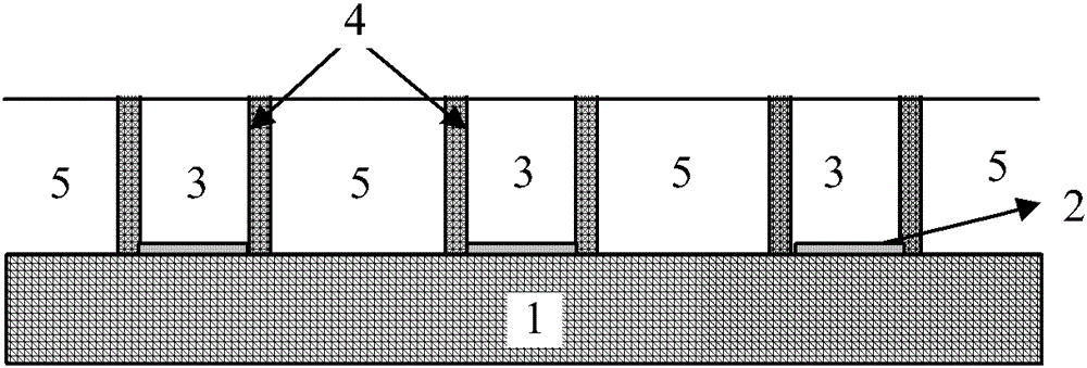
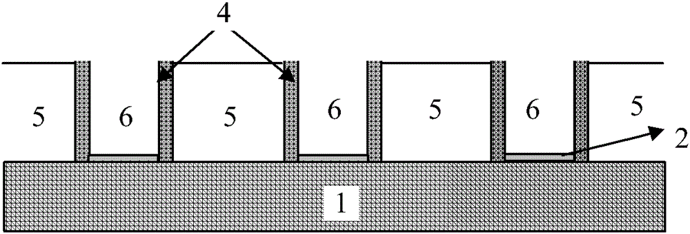
[0021] Referring to accompanying drawing 1, insulator layer 2, polysilicon dummy gate 3, gate side wall 4, interlayer dielectric layer (ILD) 5 are sequentially formed on substrate 1, then polysilicon dummy gate 3 is removed, and gate opening 6 is formed . It can be seen from FIG. 1 that after the removal of the polycrystalline dummy gate 3, the quality of the thin film of the wafer (that is, the ILD5 on the wafer surface and the sidewalls 4 sandwiched therebetween, and the thin films of the gate opening 6 The sum of mass) will be significantly reduced, so by monitoring the quality of the wafer, it can be judged whether the polycrystalline dummy gate is completely removed; the measurement by this method will have the advantages of intuitive test results, no damage to the wafer and high measurement efficiency It is suitable for the effective monitoring of the process after the polysilicon dummy gate is removed.

[0022] Specifically, a monitoring method for removing a polysilic...

Embodiment 2

[0029] Similar to Embodiment 1, a monitoring method for removing a polysilicon dummy gate in a gate-last process according to another embodiment of the present invention includes the following steps:

[0030] First, a polysilicon dummy gate structure is formed on the surface of the wafer. As shown in FIG. 1, a polysilicon dummy gate structure is formed on the surface of the wafer, that is, an insulating layer 2, a polysilicon dummy gate 3, a gate sidewall 4, and an interlayer dielectric layer (ILD) 5 are sequentially formed on a substrate 1. Then the polysilicon dummy gate 3 is removed to form a gate opening 6 .

[0031]Second, determine the measurement target and error range. The polysilicon dummy gate can be formed on the test wafer (that is, the spare wafer that is not used for final cutting into chip products) according to the process, and through this experimental design (designofexperimental, DOE) and the use of quality testing methods, it can be determined that a certa...

Embodiment 3

[0036] Similar to Embodiment 1 or 2, the only difference lies in whether the insulating layer 2 is a gate dielectric layer of the gate-last process. If the insulating layer 2 is a high-k material for the gate dielectric layer of the gate-last process, then in the monitoring method of the present invention, the insulating layer 2 is not removed along with the polysilicon dummy gate 3, but is retained together, so the monitoring method does not Change. But if the insulating layer 2 is only used for the etch stop layer of the polysilicon dummy gate 3, that is, the material is a common insulating dielectric material, such as silicon dioxide, then the insulating layer 2 should be removed together with the polysilicon dummy gate 3, then the present invention Corresponding changes need to be made in the above two embodiments.

[0037] Specifically, the monitoring method for the variation of embodiment 1 in embodiment 3 includes:

[0038] 1) Use the quality measurement monitoring me...


PUM


Abstract

Provided is a monitoring method after removing a polycrystalline silicon dummy gate, comprising the following steps: forming a polycrystalline silicon dummy gate structure on the surface of a wafer; determining the measurement objective and error range for the quality of the wafer; after removing the polycrystalline silicon dummy gate, using a quality measuring device to measure the quality of the wafer, and judging whether the polycrystalline silicon dummy gate is completely removed. The measuring method of the present invention can measure the whole wafer quickly and accurately without a specific testing structure, thus effectively monitoring and judging whether the polycrystalline silicon dummy gate is completely removed. Furthermore, the measuring method feeds back the result visually, quickly and accurately, and causes no damage to the wafer.

Description

technical field [0001] The invention relates to a manufacturing method of a semiconductor device, more specifically, to a monitoring method after removing a polysilicon dummy gate. Background technique [0002] With the successful application of high-K / metal gate engineering on the 45nm technology node, it has become an indispensable key modular project for the sub-30nm technology node. At present, only Intel, which adheres to the high-K / gatelast route, has achieved success in mass production at 45nm and 32nm. In recent years, Samsung, TSMC, Infineon and other industry giants following the IBM industry alliance have also shifted the focus of previous development from high-K / gatefirst to gatelast engineering. [0003] In the Gatelast project, after the ion high-temperature annealing is completed, the polycrystalline gate needs to be dug out, and then the metal gate electrode is filled. The process is shown in Figure 1 for details. Such as Figure 1A An insulating layer 2 , ...

Claims


Application Information

Patent Timeline
Patent Type & Authority Patents(China)
IPC IPC(8): H01L21/66
CPCH01L22/12H01L29/66545
Inventor 杨涛赵超李俊峰闫江陈大鹏
Owner INST OF MICROELECTRONICS CHINESE ACAD OF SCI
Why Eureka
Try Eureka