Wafer level chip scale package (WLCSP) multiple chip stackable packaging piece and packaging method thereof

A stacked and packaged technology, which is applied in the direction of electrical components, semiconductor devices, and electrical solid devices, can solve the problems of high precision requirements for electroplating and photolithography, complicated WLCSP production process, and high cost.

Inactive Publication Date: 2012-12-26
HUATIAN TECH XIAN
View PDF3 Cites 5 Cited by
  • Summary
  • Abstract
  • Description
  • Claims
  • Application Information

AI Technical Summary

Problems solved by technology

[0010] The traditional WLCSP production process is complicated, and the preci...

Method used


Image

  • Wafer level chip scale package (WLCSP) multiple chip stackable packaging piece and packaging method thereof

Examples


Embodiment 1

[0041] A packaging method of a WLCSP multi-chip stacked package can be carried out according to the following steps:

[0042] The first step, wafer thinning;

[0043] The thickness of wafer thinning is 50μm, and the roughness Ra is 0.10mm;

[0044] The second step is to plate metal bumps;

[0045] Plating 2um metal bumps 4 on the surface of metal Au in the chip nip area on the entire wafer;

[0046] The third step, scribing;

[0047] For wafers with a thickness below 150 μm, use a double-knife dicing machine and its process;

[0048] The fourth step is to tin-plate the corresponding area of ​​the frame;

[0049] A layer of 2um tin layer is plated on the corresponding area of ​​PAD on pin 1 in the frame;

[0050] The fifth step, on the core

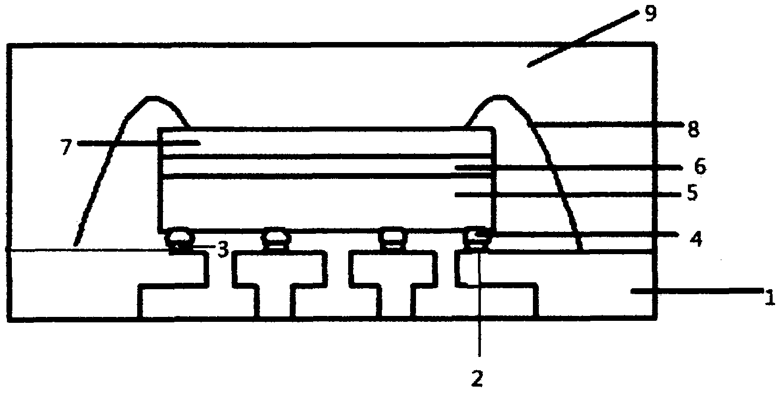
[0051] When the chip is installed, the lower IC chip 7 is turned upside down, and the bumps of the chip are welded to the frame pins by using the Flip-Chip process; the upper IC chip 5 is bonded to the lower chip 7 with the adhesive ...

Embodiment 2

[0059] A packaging method of a WLCSP multi-chip stacked package can be carried out according to the following steps:

[0060] The first step, wafer thinning;

[0061] The thickness of wafer thinning is 130μm, and the roughness Ra is 0.20mm;

[0062] The second step is to plate metal bumps;

[0063] Plating 25um metal bumps 4 on the metal Cu surface of the chip nip area on the entire wafer;

[0064] The third step, scribing;

[0065] For wafers with a thickness below 150 μm, use a double-knife dicing machine and its process;

[0066] The fourth step is to tin-plate the corresponding area of ​​the frame;

[0067] A layer of 25um tin layer is plated on the corresponding area of ​​PAD on pin 1 in the frame;

[0068] The fifth step, on the core

[0069] When the chip is installed, the lower IC chip 7 is turned upside down, and the bumps of the chip are welded to the frame pins by using the Flip-Chip process; the upper IC chip 5 is bonded to the lower chip 7 with the adhesive 6;...

Embodiment 3

[0077] A packaging method of a WLCSP multi-chip stacked package can be carried out according to the following steps:

[0078] The first step, wafer thinning;

[0079] The thickness of wafer thinning is 200μm, and the roughness Ra is 0.30mm;

[0080] The second step is to plate metal bumps;

[0081] Plating 50um metal bumps 4 on the surface of metal Au or Cu in the chip nip area on the entire wafer;

[0082] The third step, scribing;

[0083] Wafers above 150μm adopt ordinary dicing process;

[0084] The fourth step is to tin-plate the corresponding area of ​​the frame;

[0085] A layer of 50um tin layer is plated on the corresponding area of ​​PAD on pin 1 in the frame;

[0086] The fifth step, on the core

[0087] When the chip is installed, the lower IC chip 7 is turned upside down, and the bumps of the chip are welded to the frame pins by using the Flip-Chip process; the upper IC chip 5 is bonded to the lower chip 7 with the adhesive 6;

[0088] The sixth step, reflo...


PUM


Abstract

The invention relates to a wafer level chip scale package (WLCSP) multiple chip stackable packaging piece and a packaging method thereof and belongs to the technical field of integrated circuit (IC) packaging. A plastic package body surrounds pins inside a frame, an upper layer IC chip, a lower layer IC chip, dice bonding glue, a metal protruded point, a tin layer, solder and a bonding wire to form circuit integrity. The plastic package body which plays the roles of supporting and protecting the upper layer IC chip, the lower layer IC chip and the bonding wire surrounds the pins inside the frame, the tin layer, the solder, the metal protruded point and the upper layer IC chip to form the circuit integrity. The upper layer IC chip, the lower layer IC chip, the bonding wire, the metal protruded point, the solder, the tin layer and the substrate form power and signal paths of a circuit. By adopting the metallic coating protruded point different from the past and the solder to weld every protruded point of the chip with frame pins, in the process of bonding, routing is not needed, and therefore breakover and mutual connection between the chip and the pins can be achieved directly. Thus, the WLCSP multiple chip stackable packaging piece and the packaging method thereof have the advantages of being low in cost and high in efficiency.

Description

technical field [0001] The invention relates to a WLCSP multi-chip stacked package and a packaging method thereof, belonging to the technical field of integrated circuit packaging. Background technique [0002] With the rapid development of microelectronics technology and the increase in the complexity of integrated circuits, most of the functions of an electronic system may be integrated in a single chip (system on chip), which requires microelectronic packages to have higher performance and more More leads, denser interconnection, smaller size or larger chip cavity, greater heat dissipation function, better electrical performance, higher reliability, lower cost per lead, etc. The chip packaging process has changed from chip-by-chip packaging to wafer-level packaging. Wafer-level chip packaging technology——WLCSP just meets these requirements and forms a compelling WLCSP process. [0003] Wafer Level Chip Scale Packaging (WLCSP for short), that is, wafer-level chip packagin...

Claims


Application Information

Patent Timeline
IPC IPC(8): H01L23/495H01L21/60H01L25/065
CPCH01L24/73H01L2224/16245H01L2224/32145H01L2224/48247H01L2224/73253H01L2224/73265H01L2924/00012
Inventor 郭小伟蒲鸿鸣崔梦谢建友李万霞
Owner HUATIAN TECH XIAN
Why Eureka
Try Eureka