
Photoetching method for grating aided nano imaging

An optical imaging lens and grating technology, which is applied in the field of super-resolution microscopy and lithography, can solve the problems of small field of view, near field limitation, and difficult processing, and achieves the advantages of avoiding loss problems, low processing difficulty, and improving resolution. Effect

Active Publication Date: 2014-09-10
INST OF OPTICS & ELECTRONICS - CHINESE ACAD OF SCI
View PDF4 Cites 0 Cited by
  • Summary
  • Abstract
  • Description
  • Claims
  • Application Information

AI Technical Summary

Problems solved by technology

[0003] The technical problem to be solved by the present invention is: to overcome the shortcomings of conventional superdiffraction imaging lithography devices such as near-field limitation of the object image position, small field of view, and difficult processing, and proposes to use object-space gratings and image-space gratings to realize the connection between the propagating wave and the evanescent wave. The transformation between, using the optical imaging lens group to realize the projection imaging lithography method of the light field distribution

Method used


Image

  • Photoetching method for grating aided nano imaging
  • Photoetching method for grating aided nano imaging
  • Photoetching method for grating aided nano imaging

Examples


Embodiment Construction

[0015] The present invention will be described in detail below with reference to the accompanying drawings and specific embodiments, but the protection scope of the present invention is not limited to the following examples, and should include all the contents in the claims.

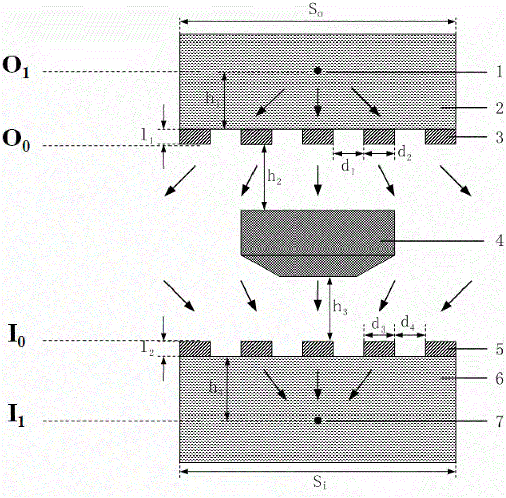
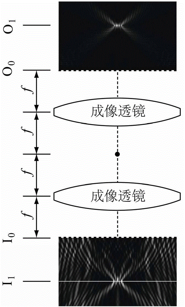
[0016] A lithography method for grating-assisted nano-imaging, the imaging device used comprises: an optical imaging lens group; an object-side grating and an image-side grating located on both sides of the optical imaging lens group; an optical lens used for projection imaging of light field distribution Group.

[0017] An object-side grating for spectral conversion is prepared under the nano-object or nano-pattern mask; an optical imaging lens group is installed under the object-side grating for projection imaging of the light field distribution; an optical imaging lens group is prepared under the optical imaging lens group for spectrum conversion Converted image square raster; the image square area is...


PUM

PropertyMeasurementUnit
sizeaaaaaaaaaa

Abstract

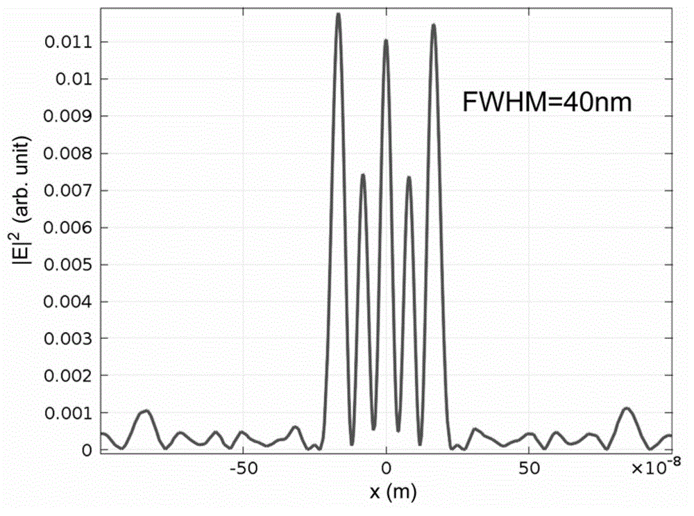
The invention provides a photoetching method for grating aided nano imaging. A nano object or a nano graphical mask is positioned in an object side region; an object side grating is placed in front of the nano object or the nano graphical mask and is used for converting a high-frequency evanescent wave into a transmission wave; an optical imaging lens group is arranged in a far field region outside the object side grating and is used for distributing, projecting and imaging the optical field; an image side grating is arranged on the other side of the optical imaging lens group and is used for converting the transmission wave into the high-frequency evanescent wave; and finally an imaging region below the image side grating is imaged. According to the photoetching method, the two gratings are used for converting the transmission wave and the evanescent wave; furthermore, the optical imaging lens group is used for distributing, projecting and imaging the optical field, so that the image of a sub-wavelength scale is obtained; the near field limitation of the conventional super-diffraction material is eliminated; an object and image space position relation can be in a far field range, and a visual field is not limited by factors such as the loss of the super-diffraction material and the processing difficulty; and the visual field can be expanded to a size which is the same as that of the visual field of the conventional imaging optical system.

Description

technical field [0001] The invention belongs to the field of super-resolution microscopic imaging and lithography, and relates to a super-resolution imaging lithography method which utilizes an optical imaging lens group to project light field distribution, and utilizes a grating to realize the transformation of transmission waves into evanescent waves. Background technique [0002] With the continuous miniaturization of semiconductor devices, the realization of nanoscale imaging lithography has become a bottleneck in the development of information science. In recent years, a super-resolution imaging device hyperlens based on artificial electromagnetic materials has been proposed, which can realize the transmission of evanescent waves, thereby obtaining super-resolution imaging lithography. However, this device has many application problems: first, the device is limited by near-field imaging, and the position of the object and the image is in a near-field relationship, which...

Claims


Application Information

Patent Timeline
Patent Type & Authority Patents(China)
IPC IPC(8): G03F7/20G02B5/18
Inventor 罗先刚王长涛赵泽宇王彦钦黄成陶兴刘玲杨磊磊蒲明薄杨欢
Owner INST OF OPTICS & ELECTRONICS - CHINESE ACAD OF SCI
Learn More