Surface plasma ultra-diffraction photoetching method based on tip-insulator-metal structure

A surface plasmon, metal probe technology, applied in the field of plasma superdiffraction lithography, can solve the problems of asymmetric light spot, high background light intensity, background interference, etc., to avoid background interference field, good focal spot uniformity, Consistent spot size

Inactive Publication Date: 2013-01-16
INST OF OPTICS & ELECTRONICS - CHINESE ACAD OF SCI
View PDF7 Cites 7 Cited by
  • Summary
  • Abstract
  • Description
  • Claims
  • Application Information

AI Technical Summary

Problems solved by technology

However, it has the disadvantage that the surface plasmon light field excited for the first time constitutes background interference and the contrast is too low
In addition, the inclined illumination used to excite SP has problems such as asymmetrical light spots, high background light intensity, prism illumination is required, and sample movement may easily lead to illumination changes.

Method used


Image

  • Surface plasma ultra-diffraction photoetching method based on tip-insulator-metal structure
  • Surface plasma ultra-diffraction photoetching method based on tip-insulator-metal structure
  • Surface plasma ultra-diffraction photoetching method based on tip-insulator-metal structure

Examples


Embodiment Construction

[0024] The implementation cases of the present invention will be introduced below with reference to the accompanying drawings, but the scope of protection of the present invention is not limited to the following embodiments, but should include all content in the claims.

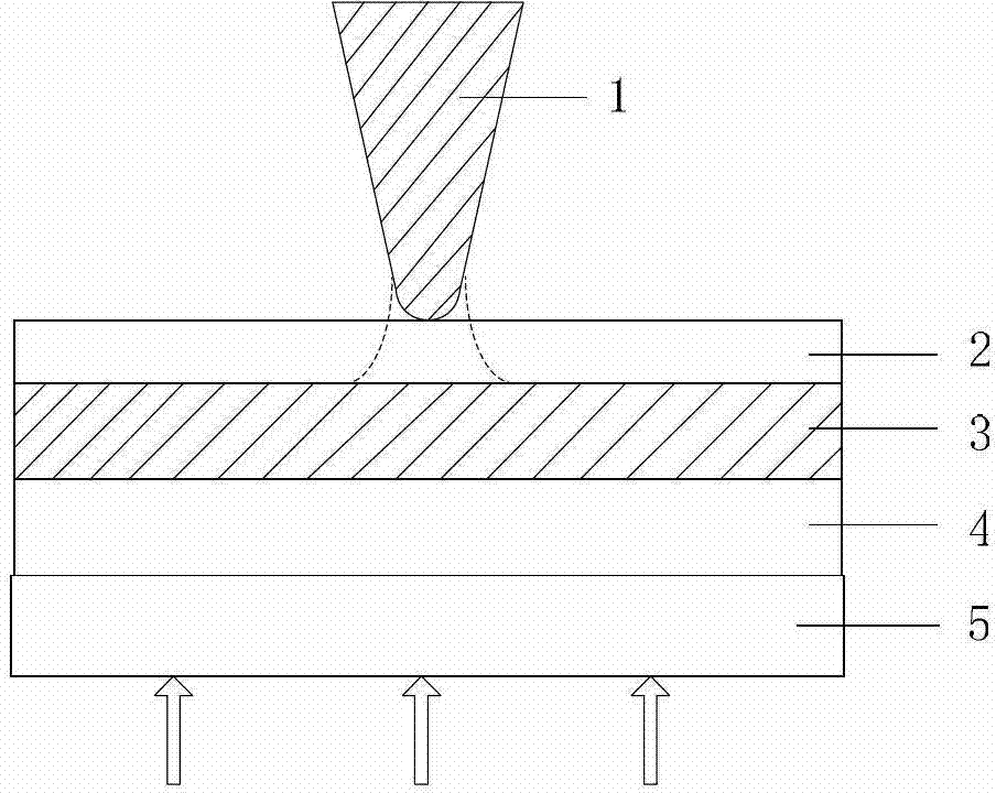
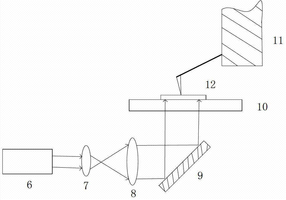
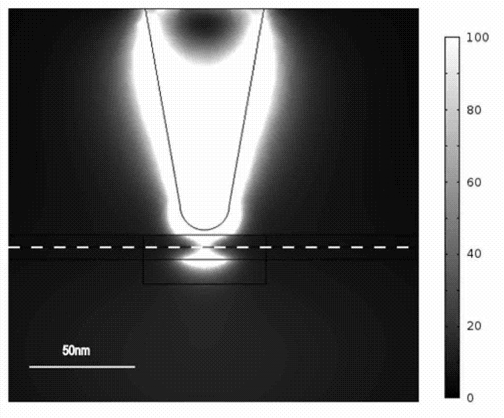
[0025] figure 1 It is a schematic diagram of the surface plasmon superdiffraction lithography method based on the metal-medium-probe (TIM) structure of the present invention, wherein the TIM structure is composed of a metal reflective layer 3 , a medium recording layer 2 and a metal probe 1 . The base can be made of transparent glass 5 , or transparent glass 5 plus dielectric material 4 . The incident light is normally incident on the TIM structure from the bottom surface of the substrate, and the localized surface plasmon is excited at the tip of the probe 1, and the localized surface plasmon is localized on the surface of the tip and decays exponentially along the longitudinal direction. Therefore, in the ...


PUM

PropertyMeasurementUnit
thicknessaaaaaaaaaa
radiusaaaaaaaaaa
thicknessaaaaaaaaaa

Abstract

The invention provides a surface plasma ultra-diffraction photoetching method based on a tip-insulator-metal (TIM) structure. The surface plasma ultra-diffraction photoetching method is characterized in that a TIM resonant cavity structure is formed by tip-insulator-metal, a light is emitted in a substrate containing the resonant cavity in a normal incidence manner, a probe tip of a probe stimulates local surface plasmas (LSP), the waves of the stimulated local surface plasmas are reflected and coupled by a metal reflection layer in a downward attenuation propagation process and reflected for multiple times to cause resonance and form relatively-uniformly-distributed regular circular light spot modes in a longitudinal distribution manner in a medium recording layer clamped between a metal reflection layer and the probe. According to the surface plasma ultra-diffraction photoetching method based on the tip-insulator-metal structure, the problem that the write-through photoetching depth of a conventional probe is shallow is solved, the sizes of the light spots (full width at half maximum, FWHM) at different depths of the medium recording layer are identical, and the energies are uniform. According to the surface plasma ultra-diffraction photoetching method, the quality of the light spot photoetched by the conventional write-through probe is greatly improved; the structure adopted by the method is simple; and the photoetching line width can be greatly reduced.

Description

technical field [0001] The invention relates to near-field direct writing lithography technology, in particular to a surface plasmon superdiffraction lithography method based on a metal-medium-probe (Tip-Insulator-Metal, TIM) structure, which can effectively improve the quality of the light spot and increase the Lithography depth Background technique [0002] With the rapid development of the information field, the structure size of optoelectronic devices is constantly shrinking, so it is urgently required that the resolution of lithography can break through the limitation of the diffraction limit. Near-field lithography is one of the important fields of research in this area in recent years. By exciting plasmons (SPPs) on the metal surface, the excited SPP wave vector is larger than the wave vector of light in vacuum to achieve the breakthrough of the diffraction limit. Purpose. Among them, probe direct writing lithography is expected to provide a low-cost, high-resolutio...

Claims


Application Information

Patent Timeline
Patent Type & Authority Applications(China)
IPC IPC(8): G03F7/20
Inventor 罗先刚王长涛赵泽宇王彦钦陶兴胡承刚高平黄成姚纳刘凯鹏
Owner INST OF OPTICS & ELECTRONICS - CHINESE ACAD OF SCI
Why Eureka
Try Eureka