Semiconductor device structure and fabrication method of semiconductor device structure

A technology of device structure and manufacturing method, which is applied in the direction of semiconductor devices, semiconductor/solid-state device manufacturing, electrical components, etc., can solve the problems of large reverse breakdown voltage, affecting device characteristics, and insufficient current handling capacity of devices, so as to improve the endurance Effect of current surge capability

Active Publication Date: 2013-01-16
SHANGHAI HUAHONG GRACE SEMICON MFG CORP
View PDF4 Cites 3 Cited by
  • Summary
  • Abstract
  • Description
  • Claims
  • Application Information

AI Technical Summary

Problems solved by technology

The carrier distribution of the P-type impurity and the carrier distribution of the N-type impurity in the P trench and the matching of the carriers of the P-type impurity and the carriers of the N-type impurity will affect the characteristics of the device, and will affect the reverse direction of the device. Breakdown Voltage and Current Handling Capability
[0003] The general device design adopts alternating P/N films to achieve the best charge balance (the total amount of P-type carriers in the P-type thin layer is equal to the total amount of N-type carriers in the N-type thin layer) to obtain the device. The largest reverse breakdown voltage, N-type epitaxy is uniformly doped, to achieve the best charge matching, the corresponding P-type thin film has a uniform doping concentration of P0, and the current handling capacity of such devices is not enough
[0004] In order to improve the current handling capability of the device, there is a way to make the P-type impurity concentration adopt an uneven distribution in the direction perpendicul

Method used


Image

  • Semiconductor device structure and fabrication method of semiconductor device structure
  • Semiconductor device structure and fabrication method of semiconductor device structure
  • Semiconductor device structure and fabrication method of semiconductor device structure

Examples


Embodiment Construction

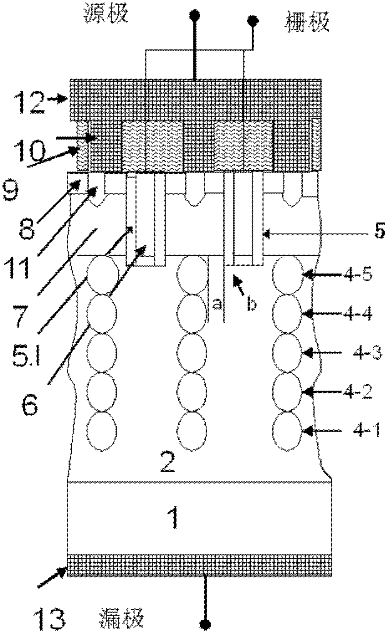
[0058] Such as figure 2 As shown, the device with a reverse breakdown voltage of 600V is an embodiment of the present invention, and the resistivity of the N+ substrate used is 0.001 ohm to 0.003 ohm. The widths of the P film and the N film are 4 microns and 8 microns in turn. N-type silicon is uniformly doped, and its doping concentration is 3E15 / CM3. In order to achieve the best charge matching, the corresponding uniform doping concentration of P-type silicon is P0 = 6E15 / CM3,

[0059] The super junction semiconductor device structure of the present invention includes:

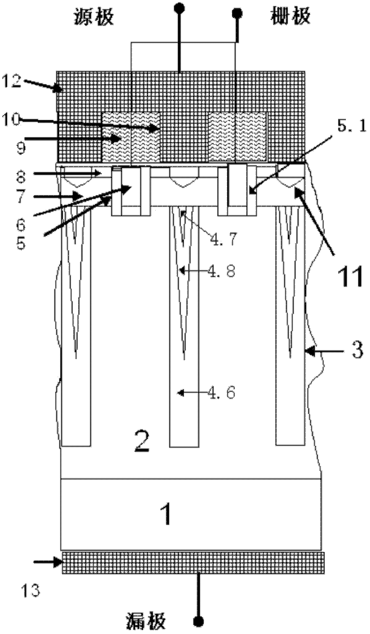
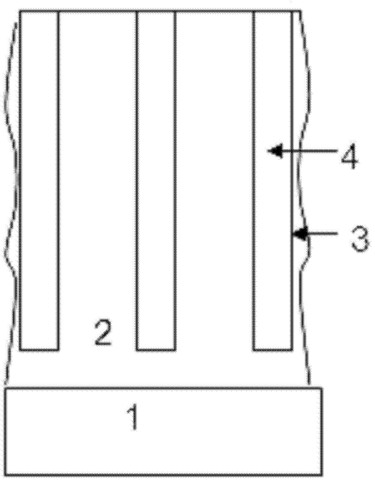
[0060] An N+ substrate (1), on which an N-type epitaxy (2) is grown, and the N-type epitaxy (2) has a plurality of P trenches (3), and the P trenches are filled with P-type silicon (4), forming a P-type film;

[0061] The top of the N-type epitaxy (2) has multiple N trenches (5), the N trenches (5) have an oxide film (5.1), and the oxide film (5.1) is filled with N-type silicon (6), forming an N-type thi...


PUM

PropertyMeasurementUnit
Thicknessaaaaaaaaaa
Thicknessaaaaaaaaaa

Abstract

The invention discloses a semiconductor device structure which comprises a substrate, a plurality of P traps and a plurality of dielectric film areas, wherein an N-type epitaxy is grown on the substrate and provided with at least one P trench filled with P-type silicon; the P traps are arranged at the top end of the N-type epitaxy; the dielectric film areas are positioned above the P traps; surface metal is installed above the dielectric film areas; a contact hole is formed between every two dielectric film areas; each P trench is at least divided into two areas; all the areas are filled with the P-type silicon in different doping concentrations; a P-type film is realized by using a nonuniform impurity distribution mode; the bottom areas of the P trenches are filled with the P-type silicon with the doping concentrations less than or equal to the uniform doping concentration; and the top middle areas of the P trenches are filled with the P-type silicon with the doping concentrations greater than the uniform doping concentration. The invention further discloses a fabrication method of the device structure. The semiconductor device structure can improve current surge resistance of a device in the switch-off process under the condition that specific on resistance of the device is not affected.

Description

technical field [0001] The invention relates to the field of semiconductor integrated circuit manufacturing, in particular to a semiconductor device structure. The invention also relates to a manufacturing method of the semiconductor device structure. Background technique [0002] The device with super junction structure replaces the N drift region in the traditional VDMOS (vertical double diffused metal-oxide semiconductor field effect transistor) through the structure of P / N alternate arrangement, combined with the well-known VDMOS process in the industry, the MOSFET with super junction structure is produced (Metal-Oxide-Semiconductor-Field-Effect Transistor), which can greatly reduce the on-resistance of the device through the low-resistivity epitaxial layer under the condition that the reverse breakdown voltage is consistent with the traditional VDMOS. The carrier distribution of the P-type impurity and the carrier distribution of the N-type impurity in the P trench and...

Claims


Application Information

Patent Timeline
IPC IPC(8): H01L29/78H01L29/06H01L21/336
Inventor 肖胜安
Owner SHANGHAI HUAHONG GRACE SEMICON MFG CORP
Why Eureka
Try Eureka