Printed circuit board, drilling method and device for printed circuit board

A technology for printed circuit boards and drilling devices, which is applied in the direction of printed circuits, printed circuits, circuit devices, etc., and can solve problems such as differences, large impact of hole link loss, and complex functions

Active Publication Date: 2015-08-26
HONOR DEVICE CO LTD
View PDF3 Cites 0 Cited by
  • Summary
  • Abstract
  • Description
  • Claims
  • Application Information

AI Technical Summary

Problems solved by technology

Due to the uneven thickness of the PCB board, there are certain differences in the thickness of the same batch of PCB boards, even the thickness of different positions of the same PCB board is also different
The disadvantage of the existing technology is that the back-drilling depth obtained according to the test results of the conventional back-drilling Coupon position on the edge of the PCB deviates from the actual depth of the back-drilling position on the PCB, and the thicker the PCB, the greater the absolute value of the deviation , the greater the deviation of the back drilling depth
[0004] The functions realized by the PCB are becoming more and more complex, and the degree of integration is getting higher and higher. Correspondingly, the PCB board needs more layers and greater thickness to meet the functional design requirements of the PCB board. The deviation of the back drilling depth obtained from the test results at the Coupon position is large, which makes the length of the stub large, and the loss of the hole link has a great impact on high-frequency signal transmission.

Method used


Image

  • Printed circuit board, drilling method and device for printed circuit board
  • Printed circuit board, drilling method and device for printed circuit board
  • Printed circuit board, drilling method and device for printed circuit board

Examples


Embodiment Construction

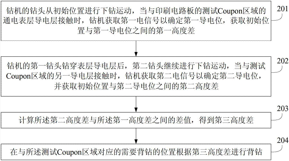
[0022] The solutions in the embodiments of the present invention will be clearly and completely described below in conjunction with the accompanying drawings in the embodiments of the present invention. Obviously, the described embodiments are only some, not all, embodiments of the present invention. Based on the embodiments of the present invention, all other embodiments obtained by persons of ordinary skill in the art without making creative efforts fall within the protection scope of the present invention.

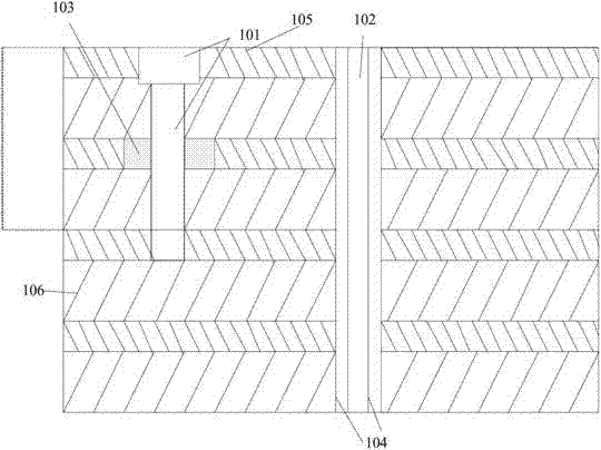
[0023] Below to figure 1 As an example to describe in detail the printed circuit board provided by the embodiment of the present invention, figure 1 A schematic cross-sectional view of a printed circuit board provided by an embodiment of the present invention.

[0024] Such as figure 1 As shown, the printed circuit board provided by the embodiment of the present invention includes a multilayer conductive layer 105 and an insulating layer 106 separating the conductive ...


PUM


Abstract

A printed circuit board, and a drilling method and device for a printed circuit board. The method comprises: a first drill of a driller conducting a drilling-down movement from an initial location, and when in contact with a surface-layer conducting layer of a test coupon region of a printed circuit board, the driller obtaining a first electrical signal so as to determine a first conducting location, and obtaining a first height difference between the initial location and the first conducting location; after the first drill of the driller drills through the surface-layer conducting layer, a second drill continuing to conduct the drilling-down movement, and when in contact with another conducting layer of the test coupon region of the printed circuit board, the driller obtaining a second electrical signal so as to determine a second conducting location, and obtaining a second height difference between the initial location and the second conducting location; calculating the difference value between the second height difference and the first height difference to obtain a third height difference; and conducting back drilling at a location which requires back drilling in accordance with the third height difference. The method achieves the aim of obtaining accurate depth information by testing a blind hole, thereby reducing the stub length for back drilling.

Description

technical field [0001] The present invention relates to the technical field of manufacturing printed circuit boards (Printed Circuit Board, PCB), in particular to a printed circuit board, a drilling method and device for the printed circuit board. Background technique [0002] With the rapid development of wireless and network communication technologies, the operating frequency of communication products is getting higher and higher, and the increase in operating frequency of communication products puts forward higher requirements for loss control in the transmission process. The back-drilling of the printed circuit board is a processing method that effectively reduces the loss of the hole link. The smaller the length of the redundant hole copper (Stub) above the signal layer after the back-drilling, the smaller the loss. [0003] Under the existing technology, the plated through hole (Plated Through Hole, PTH) is generally back-drilled according to the pre-calculated theoret...

Claims


Application Information

Patent Timeline
Patent Type & Authority Patents(China)
IPC IPC(8): H05K1/02H05K1/11H05K3/00
CPCH05K2201/09509H05K3/0047H05K1/0251H05K2203/0207
Inventor 刘山当
Owner HONOR DEVICE CO LTD
Why Eureka
Try Eureka