Supercharge Your Innovation With Domain-Expert AI Agents!

Method for removing photoresist layer

A photoresist layer and wet etching technology, applied in the semiconductor field, can solve the problems of high equipment requirements, complex process conditions, insufficient removal of the photoresist layer, etc., and achieve the effect of simple and effective removal

Inactive Publication Date: 2013-01-30
SEMICON MFG INT (SHANGHAI) CORP
View PDF9 Cites 8 Cited by
  • Summary
  • Abstract
  • Description
  • Claims
  • Application Information

AI Technical Summary

Problems solved by technology

[0006] However, the removal of the photoresist layer in the prior art is not thorough enough, which affects the subsequent process of forming semiconductor devices
[0007] In the U.S. patent of "US6627588B1", a method for removing the photoresist layer by using aliphatic alcohol is also disclosed. The process conditions of this method are complicated and the requirements for equipment are high

Method used


Image

  • Method for removing photoresist layer
  • Method for removing photoresist layer
  • Method for removing photoresist layer

Examples


Embodiment Construction

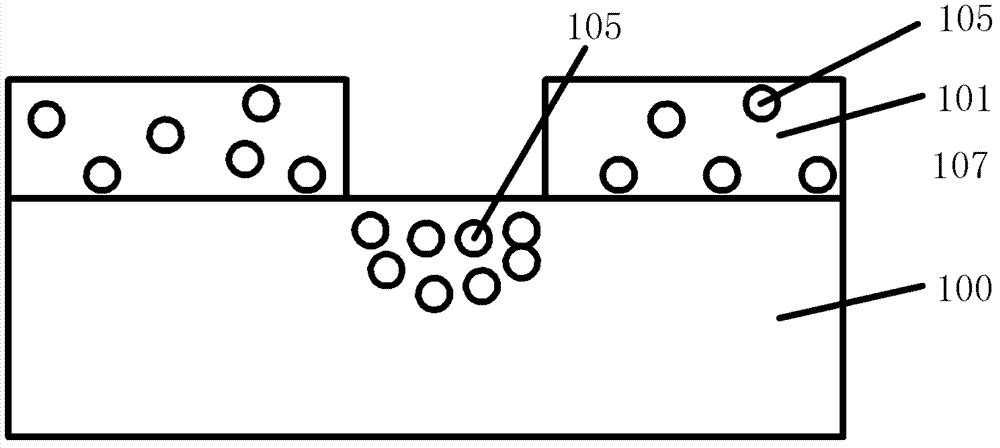
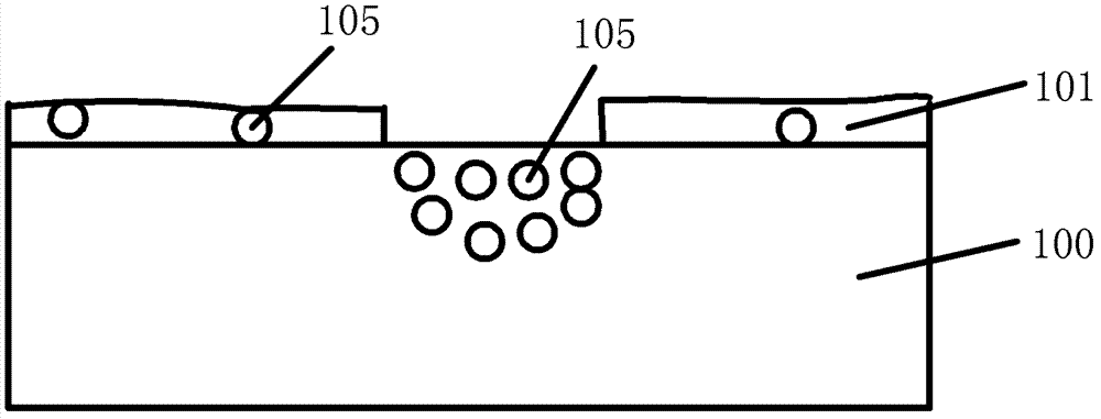
[0026] As mentioned in the background art, the method for removing the photoresist layer in the prior art does not completely remove the photoresist layer. Please continue to refer Figure 1 ~ Figure 2 , the inventor found after research that in the prior art, the photoresist layer 105 is used as a mask to implant ions 105 into the substrate 100. The photoresist layer 101 becomes hard; on the other hand, when implanting ions into the substrate 100, a part of the ions 105 stay in the photoresist layer 101; on the other hand, when implanting ions into the substrate 100, the substrate 100 Part of the silicon atoms in the photoresist layer 101 are inevitably splashed into the photoresist layer 101 under the bombardment of the ions 105; Part of the by-products produced by the reaction of the resist layer will also remain in the photoresist layer. All of the above factors will affect the removal of the photoresist layer 101 .

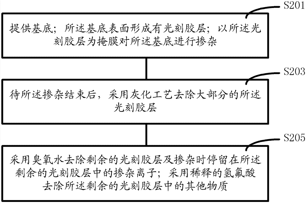
[0027] After research, the inventors found that at f...


PUM


Abstract

A method for removing photoresist layer comprises steps of: providing a substrate comprising silicon atoms, wherein substrate the surface is formed with a photoresist layer comprising at least doping ions and silicon atoms; and removing the photoresist layer by a wet etching process, wherein chemical reagents employed by the wet etching process comprise at least a first reagent for removing doping ions, and a second reagent for removing silicon atoms and / or silicon oxides. The method for removing photoresist layer in the embodiment of the invention is simple and effective, and can completely remove the photoresist layer.

Description

technical field [0001] The invention relates to the technical field of semiconductors, in particular to a method for removing a photoresist layer. Background technique [0002] In the process of forming a semiconductor device, the mask pattern on the mask plate is usually transferred to the photoresist layer on the surface of the semiconductor device by using a photolithography process, and then the mask pattern is transferred to the semiconductor device by an etching process, or in the form of The photoresist layer is used as a mask to perform ion implantation on the semiconductor device, and finally the photoresist layer is removed. [0003] In the prior art, methods for removing the photoresist layer include: [0004] Please refer to figure 1 , providing a substrate 100, the surface of the substrate 100 is formed with a photoresist layer 101; using the photoresist layer 101 as a mask to implant ions 105 into the substrate 100, the photoresist layer 101 includes ions 105...

Claims


Application Information

Patent Timeline
IPC IPC(8): G03F7/42
Inventor 刘焕新何永根
Owner SEMICON MFG INT (SHANGHAI) CORP
Features
  • R&D
  • Intellectual Property
  • Life Sciences
  • Materials
  • Tech Scout
  • Unparalleled Data Quality
  • Higher Quality Content
  • 60% Fewer Hallucinations
Learn More