
LED chip with DBR (distributed Bragg reflector) type current blocking layer and production method of LED chip

A current blocking layer, LED chip technology, applied in circuits, electrical components, semiconductor devices, etc., can solve the problems of low current utilization, weak adhesion, easy to fall off, etc., to improve current utilization, good insulation. Effect

Inactive Publication Date: 2013-01-30
SHANGHAI PN STONE PHOTOELECTRIC
View PDF4 Cites 8 Cited by
  • Summary
  • Abstract
  • Description
  • Claims
  • Application Information

AI Technical Summary

Problems solved by technology

[0007] In view of the above-mentioned shortcomings of the prior art, the object of the present invention is to provide a method to solve the weak adhesion between the current blocking layer and the highly reflective electrode in the prior art, which is easy to fall off, and the P electrode of the LED chip absorbs light. , low current utilization, etc.

Method used


Image

  • LED chip with DBR (distributed Bragg reflector) type current blocking layer and production method of LED chip
  • LED chip with DBR (distributed Bragg reflector) type current blocking layer and production method of LED chip
  • LED chip with DBR (distributed Bragg reflector) type current blocking layer and production method of LED chip

Examples


Embodiment Construction

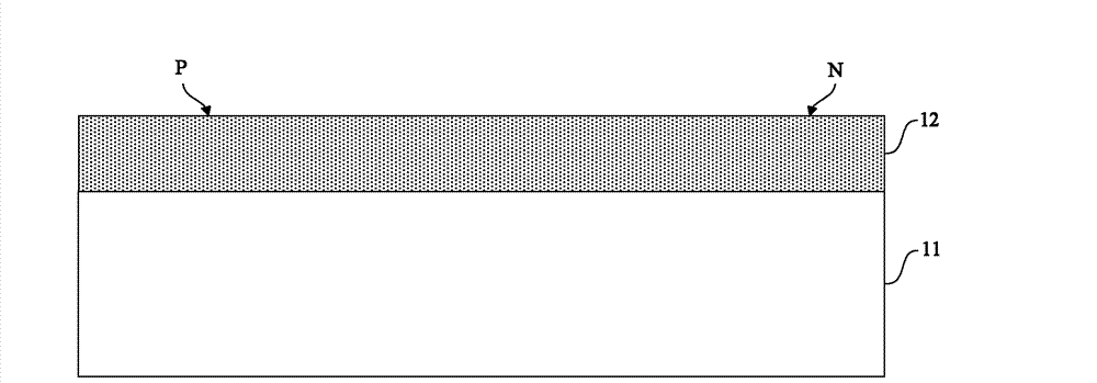
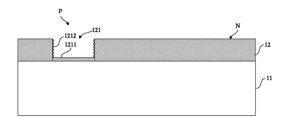
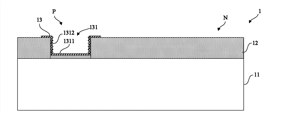
[0020] The implementation of the present invention will be illustrated by specific specific examples below, and those skilled in the art can easily understand other advantages and effects of the present invention from the content disclosed in this specification.

[0021] It should be noted that the structures, proportions, sizes, etc. shown in the drawings attached to this specification are only used to match the content disclosed in the specification, for those who are familiar with this technology to understand and read, and are not used to limit the implementation of the present invention. Limiting conditions, so there is no technical substantive meaning, any modification of structure, change of proportional relationship or adjustment of size, without affecting the effect and purpose of the present invention, should still fall within the scope of the present invention. The disclosed technical content must be within the scope covered. At the same time, terms such as "upper s...


PUM


Abstract

The invention provides an LED chip with a DBR (distributed Bragg reflector) type current blocking layer and a production method of the LED chip. The production method includes the steps: firstly, providing a sapphire substrate, forming a luminous epitaxial layer on the upper surface of the sapphire substrate, etching a groove with a waved side wall and a flat bottom surface in a P-pad region of the luminous epitaxial layer, forming a dielectric DBR on the surface of the groove to serve as the current blocking layer, and enabling the current blocking layer to form a concave structure with a waved side wall and a flat bottom surface; secondly, forming a transparent conducting layer on the luminous epitaxial layer and the concave structure, and etching the transparent conducting layer to enable the concave structure and an N region to be exposed outside; and finally, producing a P-pad on the concave structure, and producing an N-pad on the N region so that the LED chip is produced. The problems that a current blocking layer and a highly reflective electrode are low in adhesion and easy to fall off, and an LED chip is light-absorbing of a P electrode, low in current utilization rate ant the like in the prior art can be solved.

Description

technical field [0001] The invention relates to an LED chip and a manufacturing method thereof, in particular to an LED chip with a DBR type current blocking layer and a manufacturing method thereof. Background technique [0002] In the design and manufacture of LED chips, adding a current blocking layer (CBL, current blocking layer) directly under the P-pad in the LED chip can cut off the current originally flowing from the P-pad into the P-GaN layer, so that all the current flows first. Flow into the transparent conductive layer (TCL, Transparent contact layer), and then flow into the P-GaN layer directly below the transparent conductive layer through the transparent conductive layer; when no current blocking layer is added, part of the current flows from the P-pad to the transparent conductive layer first Then it flows into the P-GaN layer directly below the transparent conductive layer, and part of it directly flows into the P-GaN layer and quantum well directly below th...

Claims


Application Information

Patent Timeline
IPC IPC(8): H01L33/00H01L33/10
Inventor 林宇杰
Owner SHANGHAI PN STONE PHOTOELECTRIC
Learn More