Combined semicircular dipole printed antenna of balance microstrip line transition waveguide feed
A technology of balanced microstrip line and waveguide feeding, which is applied in the direction of resonant antenna, antenna, antenna grounding switch structure connection, etc. Achieving the effect of miniaturization
- Summary
- Abstract
- Description
- Claims
- Application Information
AI Technical Summary
Problems solved by technology
Method used
Image
Examples
specific Embodiment approach 1
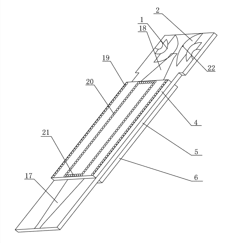
[0010] Specific implementation mode one: combine figure 1Describe this embodiment. The combined semicircular symmetrical dipole printed antenna fed by a balanced microstrip line transitional waveguide in this embodiment includes a left dipole assembly 1, a right dipole assembly 2, a transition piece 3, an upper dielectric substrate 4, Middle dielectric substrate 5, lower dielectric substrate 6, metal patch 7 on the upper dielectric substrate, metal patch 8 on the upper dielectric substrate, metal patch 9 on the lower dielectric substrate, metal patch 10 on the lower dielectric substrate, The metal patch 11 on the middle dielectric substrate, the metal patch 12 under the middle dielectric substrate, the metal strips 13 under the two upper dielectric substrates, the metal strips 14 on the two middle dielectric substrates, the metal strips under the two middle dielectric substrates Strip 15, two metal strips 16 on the lower dielectric substrate, two long balanced microstrip lines...
specific Embodiment approach 2
[0014] Specific implementation mode two: combination Figure 7 to Figure 8 To illustrate this embodiment, the balanced microstrip line transitional waveguide-fed combined semicircular symmetrical dipole printed antenna described in this embodiment is respectively provided with an extended boss 5-1 on both sides of the other end of the middle dielectric substrate 5 . The technical effect of this embodiment is that only increasing the size of the dielectric plate in the vibrator region is beneficial to reducing the total area of the dielectric plate. Other components and connections are the same as those in the first embodiment.
specific Embodiment approach 3
[0015] Specific implementation mode three: combination Figure 5 to Figure 10 Describe this embodiment, the length of the upper dielectric substrate 4 of the combined semicircular symmetrical dipole printed antenna fed by the balanced microstrip line transitional waveguide described in this embodiment is 50mm, the width of the upper dielectric substrate 4 is 35mm, and the upper dielectric The thickness of the substrate 4 is 1.5mm, the length of the middle dielectric substrate 5 is 120mm, the width of one end of the middle dielectric substrate 5 is 35mm, the width of the other end of the middle dielectric substrate 5 is 38mm, and the thickness of the middle dielectric substrate 5 is 1.5mm, the length of each extended boss 5-1 of the middle dielectric substrate 5 is 25mm, the length of the lower dielectric substrate 6 is 50mm, the width of the lower dielectric substrate 6 is 35mm, and the thickness of the lower dielectric substrate 6 is 1.5mm, the length of the metal patch 11 on...
PUM
| Property | Measurement | Unit |
|---|---|---|
| Length | aaaaa | aaaaa |
| Width | aaaaa | aaaaa |
| Thickness | aaaaa | aaaaa |
Abstract
Description
Claims
Application Information


