Etching method for improving bottom of silicon carbide table board

A silicon carbide, mesa technology, applied in the direction of electrical components, semiconductor/solid-state device manufacturing, circuits, etc., to achieve the effect of easy operation, improved etching method, and smooth surface

Active Publication Date: 2013-02-06
NO 55 INST CHINA ELECTRONIC SCI & TECHNOLOGYGROUP CO LTD
View PDF6 Cites 9 Cited by
  • Summary
  • Abstract
  • Description
  • Claims
  • Application Information

AI Technical Summary

Problems solved by technology

[0004] The present invention proposes an etching method for improving the bottom of silicon carbide mesa, the purpose of which is to improve the bottom state of silicon carbide mesa of different heights by optimizing the etching conditions, improve the surface smoothness and solve the problem of waves and beaks at the bottom of the mesa , edge grooves, etc.

Method used


Image

  • Etching method for improving bottom of silicon carbide table board
  • Etching method for improving bottom of silicon carbide table board
  • Etching method for improving bottom of silicon carbide table board

Examples


Embodiment 1

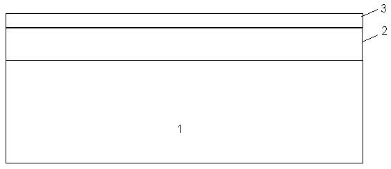
[0022] Process step 1, a layer of dielectric film 3 is formed on the silicon carbide epitaxial layer 2 by chemical vapor deposition, such as figure 1 As shown; the silicon carbide epitaxial layer 2 is a silicon carbide wafer, or an epitaxial layer in which one or more layers of silicon carbide films are grown on the silicon carbide substrate 1 . The chemical vapor deposition method used is inductively coupled plasma enhanced chemical vapor deposition (ICP-PECVD) or plasma enhanced chemical vapor deposition (PECVD).

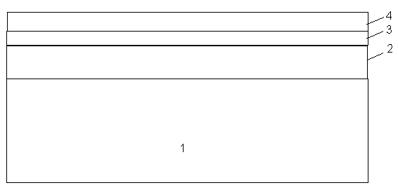
[0023] Process step 2, coating photoresist 4 on dielectric film 3, such as figure 2 shown.

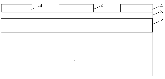
[0024] The third process step is to form the pattern transfer of the mesa through the photolithography process, such as image 3 shown.

[0025] Process step 4, the photoresist 4 is used as a barrier layer, and the dielectric film 3 is dry-etched using the first condition, such as Figure 4 shown.

[0026] The first conditional dry etching dielectric film 3 process i...

Embodiment 2

[0047] Process step 1, a layer of dielectric film 3 is formed on the silicon carbide epitaxial layer 2 by chemical vapor deposition, such as figure 1 As shown; the silicon carbide epitaxial layer 2 is a silicon carbide wafer, or an epitaxial layer in which one or more layers of silicon carbide films are grown on the silicon carbide substrate 1 . The chemical vapor deposition method used is inductively coupled plasma enhanced chemical vapor deposition (ICP-PECVD) or plasma enhanced chemical vapor deposition (PECVD).

[0048] Process step 2, coating photoresist 4 on dielectric film 3, such as figure 2 shown.

[0049] The third process step is to form the pattern transfer of the mesa through the photolithography process, such as image 3 shown.

[0050] Process step 4, the photoresist 4 is used as a barrier layer, and the dielectric film 3 is dry-etched using the first condition, such as Figure 4 shown.

[0051] The first conditional dry etching dielectric film 3 process i...

Embodiment 3

[0072] Process step 1, a layer of dielectric film 3 is formed on the silicon carbide epitaxial layer 2 by chemical vapor deposition, such as figure 1 As shown; the silicon carbide epitaxial layer 2 is a silicon carbide wafer, or an epitaxial layer in which one or more layers of silicon carbide films are grown on the silicon carbide substrate 1 . The chemical vapor deposition method used is inductively coupled plasma enhanced chemical vapor deposition (ICP-PECVD) or plasma enhanced chemical vapor deposition (PECVD).

[0073] Process step 2, coating photoresist 4 on dielectric film 3, such as figure 2 shown.

[0074] The third process step is to form the pattern transfer of the mesa through the photolithography process, such as image 3 shown.

[0075] Process step 4, the photoresist 4 is used as a barrier layer, and the dielectric film 3 is dry-etched using the first condition, such as Figure 4 shown.

[0076] The first conditional dry etching dielectric film 3 process i...


PUM


Abstract

The invention relates to an etching method for improving the bottom of a silicon carbide table board. The technique comprises the following steps: 1, a layer of dielectric film is formed on an outward-extending silicon carbide layer; 2, photoresist is coated on the dielectric film, so as to form pattern transfer of the table board through a photolithography technique; 3, the photoresist serves as a barrier layer, and the dielectric film is etched by the dry method under a first condition; 4, the photoresist out of the etched dielectric film on the surface of silicon carbide can be removed at the same time; 5, the remaining dielectric film serves as a barrier layer, and the silicon carbide is etched by the dry method under a second condition to form the table board; and 6, after part of the processes, all dielectrics on the surface of the silicon carbide can be removed through wet etching. The etching method has the advantages that the problems of burrs at edges when a metal mask forms the silicon carbide table board, peaks caused by the slight sputtering of metal, metal ion pollution easily caused at high temperature and the like can be solved, and the injection protection for the silicon carbide table board as well as the exposure and the etching of the area out of the table board can be ensured through a self-alignment mode, so that the surface of the bottom area of the table board can be smooth, and the subsequent process operation can be convenient.

Description

technical field [0001] The invention relates to a method for forming a smooth bottom of a self-aligned mesa, in particular to an etching method for improving the bottom of a silicon carbide mesa. Background technique [0002] Silicon carbide (SiC), a wide bandgap semiconductor material, has the characteristics of wide bandgap width, high critical field strength, high thermal conductivity, and high carrier saturation rate. SiC epitaxy on SiC substrate is the most important semiconductor material for manufacturing high temperature, high frequency, high power devices, etc. It has super performance and broad application prospects. In SiC microwave and power electronic devices, the mesa structure is commonly used in Schottky diodes, static induction transistors, junction field effect transistors, etc., so how to make a smooth bottom of the mesa without waves and bird’s beak problems so as to form a good coverage The gate metal is a key method to achieve device performance and re...

Claims


Application Information

Patent Timeline
Patent Type & Authority Applications(China)
IPC IPC(8): H01L21/04
Inventor 陈刚李理刘海琪柏松
Owner NO 55 INST CHINA ELECTRONIC SCI & TECHNOLOGYGROUP CO LTD
Why Eureka
Try Eureka