
Non-volatile storage device and method for manufacturing the same

A non-volatile storage and manufacturing method technology, applied in the field of non-volatile storage devices, can solve the problems of reduced stress migration resistance, easy migration, and increased stress variation, so as to improve the stress migration resistance and stabilize the memory Characteristics, effect of resistance change stabilization

Inactive Publication Date: 2013-02-06
PANASONIC SEMICON SOLUTIONS CO LTD
View PDF6 Cites 0 Cited by
  • Summary
  • Abstract
  • Description
  • Claims
  • Application Information

AI Technical Summary

Problems solved by technology

The Cu wiring near the hole of the memory cell is damaged by etching when forming the hole, so the resistance to stress migration is reduced
In addition, the wiring of the cross-point memory is linear and long, so there is a concern that the amount of stress change will increase and migration may occur locally.
If a void is generated, the wiring resistance increases and its variation also increases, which is a fatal problem for cross-point memory devices that are extremely sensitive to changes in wiring resistance

Method used


Image

  • Non-volatile storage device and method for manufacturing the same
  • Non-volatile storage device and method for manufacturing the same
  • Non-volatile storage device and method for manufacturing the same

Examples


Embodiment approach 1

[0061] [Structure of variable resistance nonvolatile memory device]

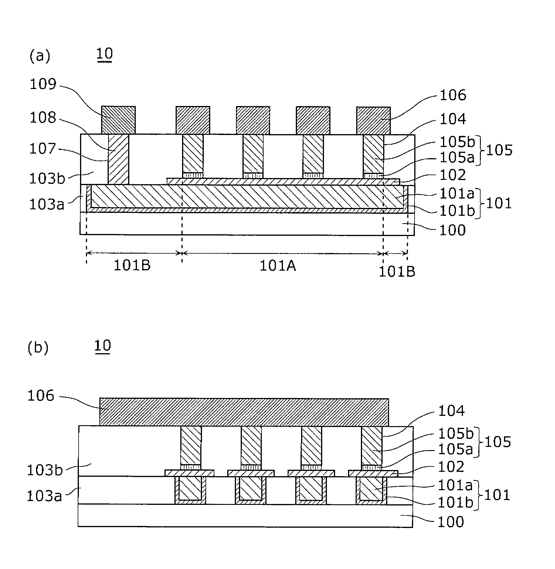
[0062] figure 1 It is a plan view showing a structural example of the nonvolatile memory device 10 according to Embodiment 1 of the present invention (the following nonvolatile memory devices 20 , 30 , 40 , 50 , and 60 have the same structure in plan view). figure 2 (a) means viewing along the direction of the arrow figure 1 The cross-sectional view of the single-dot dash line part shown in 1A-1A', figure 2 (b) means viewing along the direction of the arrow figure 1 The cross-sectional view of the single-dot dash line part shown in 1B-1B' in .

[0063] Such as figure 1 with figure 2 As shown, the first wiring 101 and the second wiring 106 each have a line shape and cross each other through the second interlayer insulating layer 103b. A memory cell hole 104 is formed penetrating through the second interlayer insulating layer 103 b at the intersection position, and a variable resistance element is...

Embodiment approach 2

[0105] [Structure of variable resistance nonvolatile memory device]

[0106] Figure 8 (a) and (b) are cross-sectional views showing a configuration example of the resistance variable nonvolatile memory device 30 according to Embodiment 2 of the present invention. Figure 8 (a) means viewing along the direction of the arrow figure 1 The cross-sectional view of the single-dot dash line part shown in 1A-1A', Figure 8 (b) means viewing along the direction of the arrow figure 1 The cross-sectional view of the single-dot dash line part shown in 1B-1B' in .

[0107] Among them, there are the following two points of difference from the nonvolatile memory device 10 of the first embodiment.

[0108] The first point is that the end face of the first electrode 102 made of noble metal and the end face of the first wiring 101 are located in the same plane in the direction perpendicular to the cross section of the line 1B-1B' (see Figure 8 (b)). The first electrode 102 and the fir...

Embodiment approach 3

[0122] Figure 13 (a) and (b) are cross-sectional views showing a configuration example of the resistance variable nonvolatile memory device 40 according to Embodiment 3 of the present invention. Figure 13 (a) means viewing along the direction of the arrow figure 1 The cross-sectional view of the single-dot dash line part shown in 1A-1A', Figure 13 (b) means viewing along the direction of the arrow figure 1 The cross-sectional view of the single-dot dash line part shown in 1B-1B' in .

[0123] The difference from the nonvolatile memory device 10 of Embodiment 1 is that the first variable resistance layer 105 a of the variable resistance element is formed not only on the bottom of the memory cell hole 104 but also on the sidewall. The first variable resistance layer 105 a is formed in a ring shape along the inner wall (side wall) of the memory cell hole 104 when viewed from a plan view, and the second variable resistance layer 105 b is formed inside it.

[0124] The fir...


PUM


Abstract

Disclosed is a variable-resistance non-volatile storage device which varies resistance in a stable manner and is adapted for miniaturization. The non-volatile storage device comprises: a first wiring (101) formed by a barrier metal layer (101b) which covers the bottom face and the side face of a wiring groove formed in a first inter-layer insulation layer (103a), and by a main layer (101a) that fills the interior of the wiring groove; a first electrode (102) made of a noble metal and covering the upper surface of the first wiring (101); a plurality of memory cell holes (104) formed in a second inter-layer insulation layer (103b); a resistance varying layer (105) formed in the memory cell holes (104) and connected to the first electrode (102); and a second wiring (106) covering the resistance varying layer (105) and the memory cell holes (104). In a region (101A) in the vicinity of the memory cell holes (104), the main layer (101a) is encompassed by the barrier metal layer (101b) and the first electrode (102) in an arbitrary cross section in the width direction of the first wiring (101).

Description

technical field [0001] The present invention relates to a nonvolatile memory device having a variable resistance element whose resistance value is stably held and changed by application of a voltage pulse. Background technique [0002] In recent years, with the development of digital technology, electronic devices such as portable information devices and information home appliances have further achieved higher functionality. Along with the high functionality of these electronic devices, the miniaturization and speed-up of semiconductor elements used are rapidly progressing. Among them, applications of large-capacity nonvolatile memories represented by flash memory are rapidly expanding. In addition, as a next-generation new nonvolatile memory to replace the flash memory, a nonvolatile memory device using a variable resistance element (variable resistance nonvolatile memory device, or simply referred to as a nonvolatile memory device) is being promoted. ) development. Here...

Claims


Application Information

Patent Timeline
Patent Type & Authority Applications(China)
IPC IPC(8): H01L27/105H01L21/3205H01L27/10H01L45/00H01L49/00H10B99/00
CPCH01L21/76807H01L27/101H01L45/1625H01L45/1616H01L27/2409H01L45/08H01L27/2481H01L27/2463H01L45/146G11C2213/51H01L45/1683H01L21/76849H01L45/1233G11C13/0007H10B63/20H10B63/80H10B63/84H10N70/24H10N70/826H10N70/8833H10N70/026H10N70/066
Inventor 三河巧空田晴之
Owner PANASONIC SEMICON SOLUTIONS CO LTD
Learn More