Method for removing parylene film layer on surface of PCBA

A technology of parylene and film layer, which is applied in the field of removal of parylene film layer on the surface of PCBA board, can solve the problems of damaged PCBA board, expensive laser equipment, high cost of film removal, etc., achieves low cost, simple method and reduced production cost effect

Pending Publication Date: 2021-09-07
SHENZHEN AOLAN TECH CO LTD
View PDF7 Cites 0 Cited by
  • Summary
  • Abstract
  • Description
  • Claims
  • Application Information

AI Technical Summary

Problems solved by technology

How to ensure that there is no film layer at the welding position? The usual usage is glue dispensing, that is, put UV glue on the position where the pad needs to be welded, and then remove the UV glue after the coating is completed, but before removing the UV glue, you need to use a laser or a blade to remove the UV glue around the UV glue. Make a cut to avoid lifting the surrounding film layer when removing the UV glue. This method is complicated and has the risk of damaging the PCBA board
Another method is to use a laser to remove the parylene film on the welding pad, but the laser equipment is expensive and the film removal cost is high

Method used

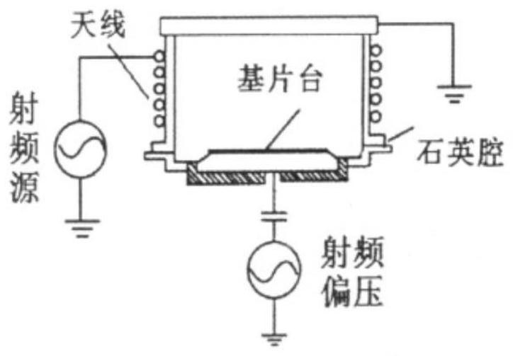
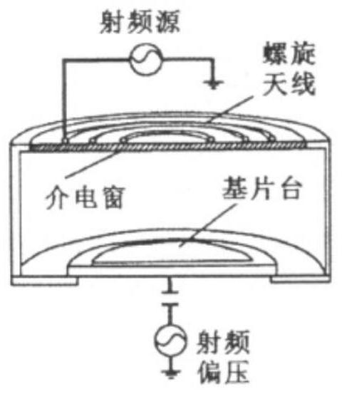
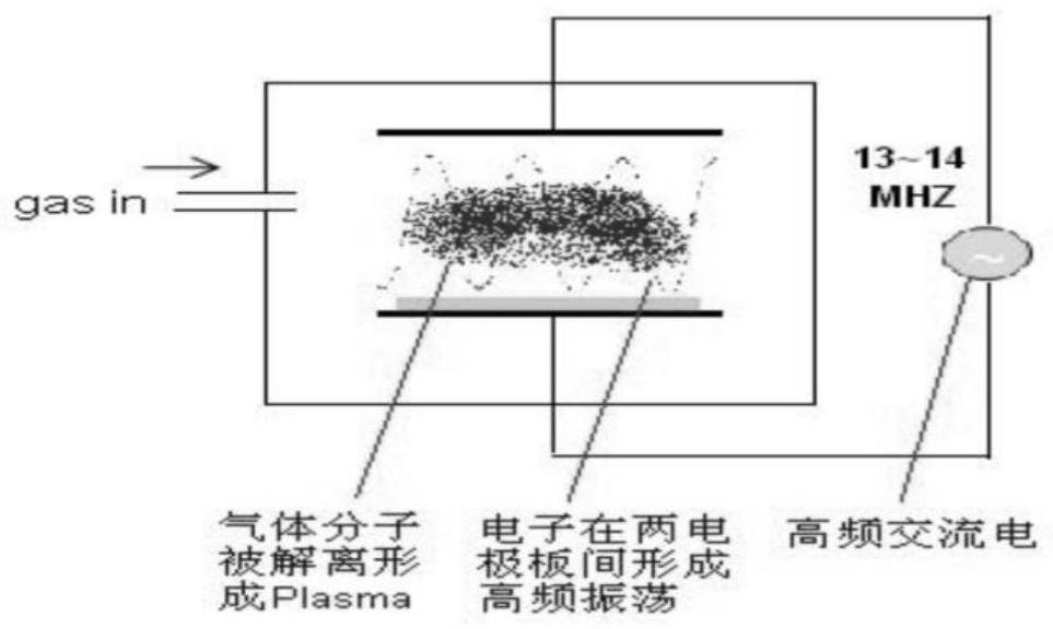

Image

  • Method for removing parylene film layer on surface of PCBA
  • Method for removing parylene film layer on surface of PCBA
  • Method for removing parylene film layer on surface of PCBA

Examples


Embodiment 1

[0057] The method for removing the parylene film on the surface of the PCBA board of the present embodiment is as follows:

[0058] (1) PCBA board is provided. The surface of the PCBA board is provided with a parylene N-type film layer. The parylene film layer has a preset area to be removed, and the thickness of the parylene film layer in the area to be removed is 8 μm

[0059] (2) Cover the PCBA board with a shielding cover, the material of the shielding cover is Teflon, and the shielding cover is provided with a through hole, and the position of the through hole corresponds to the position of the area to be removed.

[0060] (3) Perform plasma etching on the above-mentioned PCBA board in the flat PECVD system, under the protection of the mask, only the parylene film layer at the corresponding position of the through hole is etched. During the etching process, no bias power supply and inductor are added, the oxygen flow rate is 250sccm, and the fluorine-containing gas CF 4 ...

Embodiment 2

[0063] The method for removing the parylene film on the surface of the PCBA board of the present embodiment is as follows:

[0064] (1) A PCBA board is provided, and the surface of the PCBA board is provided with a parylene N-type film layer. The parylene film layer has a preset area to be removed, and the thickness of the parylene film layer in the area to be removed is 8 μm.

[0065] (2) Cover the PCBA board with a shielding cover, the material of the shielding cover is TPU, and the shielding cover is provided with a through hole, and the position of the through hole corresponds to the position of the area to be removed.

[0066] (3) In the flat PECVD system, the above-mentioned PCBA board is plasma etched. During the etching process, no bias power supply and inductor are added, the oxygen flow rate is 250 sccm, and the fluorine-containing gas CF 4 The flow rate is 40sccm, the flow rate of argon gas is 0, the radio frequency power is 450W, and the working pressure is 32Pa. ...

Embodiment 3

[0069] The method for removing the parylene film on the surface of the PCBA board of the present embodiment is as follows:

[0070] (1) A PCBA board is provided, and the surface of the PCBA board is provided with a parylene N-type film layer. The parylene film layer has a preset area to be removed, and the thickness of the parylene film layer in the area to be removed is 8 μm.

[0071] (2) Cover the PCBA board with a shielding cover, the material of the shielding cover is Teflon, and the shielding cover is provided with a through hole, and the position of the through hole corresponds to the position of the area to be removed.

[0072](3) Perform plasma etching on the above-mentioned PCBA board in a flat PECVD system. During the etching process, no bias power supply and inductor are added, the oxygen flow rate is 250 sccm, and the fluorine-containing gas SF 6 The flow rate is 63sccm, the flow rate of argon gas is 0, the radio frequency power is 450W, and the working pressure is...


PUM


Abstract

The invention relates to a method for removing a parylene film layer on the surface of a PCBA. The method comprises the following steps: providing the PCBA, wherein the parylene film layer is arranged on the surface of the PCBA, and the parylene film layer is provided with a preset to-be-removed area; arranging a shielding cover on the PCBA board in a covering mode, and forming a through hole in the shielding cover, wherein the position of the through hole corresponds to the position of the to-be-removed area; carrying out the plasma etching on the parylene film layer, in the etching process, not adding a bias power supply and an inductor, wherein the flow ratio of fluorine-containing gas to oxygen in the etching process is controlled to be (0.3-0.5): 1, and the radio frequency power is 450-1000 W. According to the etching method of the parylene film layer, the radio frequency power is improved, the flow ratio of CF4 to O2 is adjusted at the same time, rapid etching of the parylene film layer is achieved under the condition that a bias power supply and an inductor are not needed, and the production cost is reduced.

Description

technical field [0001] The invention relates to the field of etching, in particular to a method for removing a parylene film layer on the surface of a PCBA board. Background technique [0002] Parylene is a new type of coating material developed in the mid-1960s, which is a polymer of p-xylene. The CVD (Chemical Vapor Deposition) method can produce a uniform thickness, dense pinhole-free, transparent parylene film (parylene film) that can cover all surfaces, including the smallest corners or cracks, sharp edges or surface ripples. These properties position parylene as an ideal protective coating for use in aerospace, medical and microelectromechanical systems (MEMS), among other fields. However, when the parylene film layer is prepared by CVD, partial shielding is sometimes required. For example, the conductivity of the place that needs to be welded will become poor after the parylene film layer is covered, so it needs to be protected. How to ensure that there is no film ...

Claims


Application Information

Patent Timeline
Patent Type & Authority Applications(China)
IPC IPC(8): H05K3/22
CPCH05K3/22
Inventor 吕勇云洋
Owner SHENZHEN AOLAN TECH CO LTD
Why Eureka
Try Eureka